


Chapter 1
Introduction
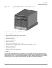
Detailed hp rp7405/rp7410 Description
11
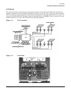
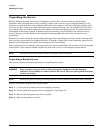
System Backplane
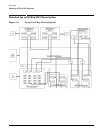
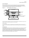
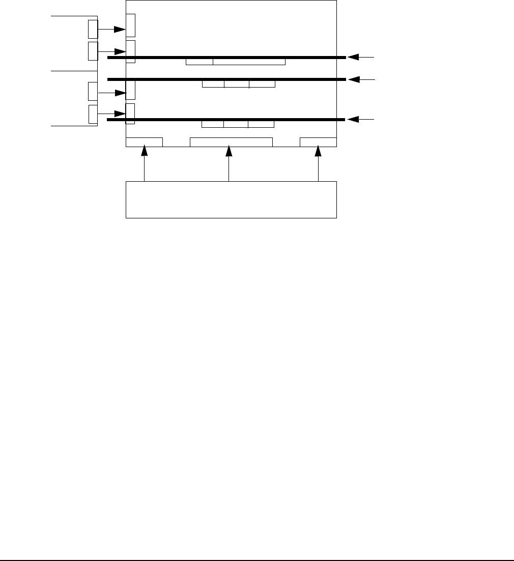
The system backplane comprises the system clock generation logic, the system reset generation logic,
DC-to-DC converters, power monitor logic, and two LBA link-to-PCI converter ASICs. It also includes
connectors for attaching the cell boards, PCI backplane, MP Core I/O MP/SCSI boards, SCSI cables, bulk
power, chassis fans, front panel display, intrusion switches, and the system scan card.
Figure 1-8 System Backplane Block Diagram
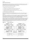
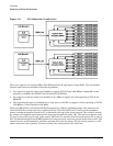
Only half of the MP Core I/O board set connects to the system backplane. The MP/SCSI boards plug into the
backplane, while the LAN/SCSI boards plug into the PCI backplane.
Clocks and Reset
The system backplane contains reset and clock circuitry that propagates through the whole system. The
central clocks drive all major chip set clocks. Therefore, these circuits represent a system wide single point of
failure.
I/O Subsystem
The cell board-to-I/O path runs from the CC to the SBA, from the SBA to the ropes, from the ropes to the LBA,
and from the LBA to the PCI buses. The CC on each cell board communicates with one SBA over the SBA
link. The SBA link consists of both an inbound and an outbound link with an effective bandwidth of
approximately 1 GB/sec. The SBA converts the SBA link protocol into “ropes.” The SBA can support up to 16
of these high-speed bi-directional rope links for a total aggregate bandwidth of approximately 4 GB/sec. The
LBA acts as a bus bridge, supporting either one or two ropes and capable of driving either PCI-2x Turbo (33
MHz x 64 bits) or PCI-4 Twin Turbo (66 MHz x 64 bits) respectively
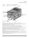
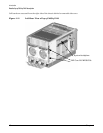
PCI backplane
Cell board 0
Cell board 1
System backplane
Bulk power supply
MP Core I/O
MP/SCSI
MP Core I/O
MP/SCSI
Cell boards are perpendicular
to the system backplane.