I/O Subsystem Intel® Server Board SDS2
Revision 1.2
Order Number: A85874-002
20
4.6.2 BIOS Flash
The SDS2 Server Board incorporates a Fairchild* 29LV008B 8Mbit Flash ROM. The flash device
is connected through the X-bus of the CSB5.
4.7 Interrupt Routing
The SDS2 Server Board interrupt architecture implements both PC-compatible PIC mode and
APIC mode interrupts through the use of the integrated I/O APICs in the CSB5.
4.7.1 Legacy Interrupt Routing
For PC-compatible mode, the CSB5 provides two 82C59-compatible interrupt controllers. The
two controllers are cascaded with interrupt levels 8-15 entering on level 2 of the primary interrupt
controller (standard PC configuration). A single interrupt signal is presented to the processors, to
which only one processor will respond for servicing. The CSB5 contains configuration registers
that define which interrupt source logically maps to I/O APIC INTx pins.
Interrupts, both PCI and IRQ types, are handled by the CSB5. The CSB5 then translates these to
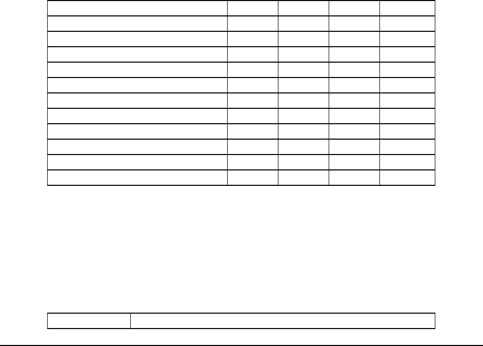
the APIC bus. The numbers in the table below indicate the CSB5 PCI interrupt input pin to which
the associated device interrupt (INTA, INTB, INTC, INTD) is connected. The CSB5’s I/O APIC
exists on the I/O APIC bus with the processors.
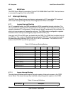
Table 12. PCI Interrupt Routing/Sharing
Interrupt Device INTA INTB INTC INTD
ATI RAGE XL 4
82550PM #1 2
82550PM #2 3
PCI Slot 1 (P64-B) 5 13 11 12
PCI Slot 2 (P64-B) 6 12 13 11
PCI Slot 3 (P32-A) 7 11 12 13
PCI Slot 4 (P32-A) 8 13 11 12
PCI Slot 5 (P64-C) 9 12 13 11
PCI Slot 6 (P64-C) 10 11 1 0
7899W-SCSI Ch A 0
7899W-SCSI Ch B 1
4.7.1.1 Legacy Interrupt Routing
The table below recommends the logical interrupt mapping of interrupt sources on the SDS2
Server Board. The actual interrupt map is defined using configuration registers in the CSB5.
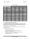
Table 13. Interrupt Definitions
ISA Interrupt Description


