


– 88 –
APPENDIX D
PCI-1712/1712L User’s Manual
Advantech Co., Ltd.
www.advantech.com
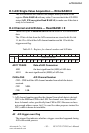
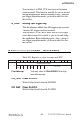
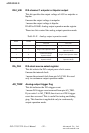
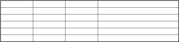
Table D-7: Analog Input Acquisition Mode
AD_CLK A/D sample clock source select register
This bit is used to select the A/D sample clock source.
0 means internal clock.
1 means external clock (from pin AI_CLK).
AD_TR Trigger source control register
This bit is used to select the A/D conversion trigger source.
0 means external digital TTL-trigger (from pin AI_TRG).
1 means threshold analog trigger (from pin ANA_TRG).
AD_TRE Trigger edge control register
This bit specifies the type of trigger edge for A/D conver
sion.
0 means rising edge.
1 means falling edge.
AIO_CAL Analog I/O calibration bit
This bit sets the Analog I/O calibration mode.
0 means the PCI-1712 is in normal mode. All analog input
channels are connected to 68 pin SCSI-II connector
respectively.
1 means the PCI-1712 is in AI/O calibration mode. The
wiring becomes that AI0 is connected to 0 V (AGND), AI2
is connected to +5 V, AI4 is connected to AO0, and AI6 is
connected to AO1 automatically.
DMA_TCF DMA terminal count flag
This bit indicates if the DMA counter is terminal count.
1 means terminal count of DMA counter occurred.
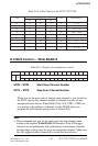
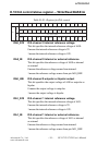
2MDA 1MDA 0MDA gninaeM
0 0 0 edoMnoitisiuqcAeulaVelgniS
0 0 1 edoMnoitisiuqcArecaP
0 1 0 edoMnoitisiuqcAreggirT-tsoP
0 1 1 edoMnoitisiuqcAreggirT-yaleD
1 0 0 edoMnoitisiuqcAreggirT-tuobA