


– 85 –
APPENDIX D
PCI-1712/1712L User’s Manual
Advantech Co., Ltd.
www.advantech.com
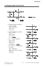
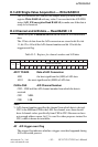
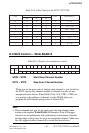
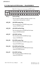
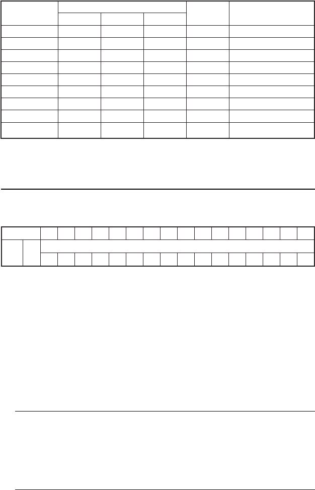
U/B
edoCniaG
niaG )V(egnaRtupnI
2G 1G 0G
0 0 0 0 1 5+~5-
0 0 0 1 2 5.2+~5.2-
0 0 1 0 4 52.1+~52.1-
0 0 1 1 8 526.0+~526.0-
0 1 0 0 5.0 01+~01-
1 0 0 0 1 01~0
1 0 0 1 2 5~0
1 0 1 0 4 5.2~0
1 0 1 1 8 52.1~0
Table D-4: Gain Codes for the PCI-1712/1712L
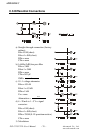
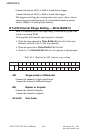
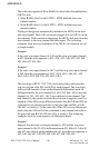
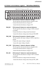
D.6 MUX Control Write BASE+4
Table D-5: Register for multiplexer control
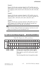
STR3 ~ STR0 Start Scan Channel Number
STP3 ~ STP0 Stop Scan Channel Number
When you set the gain code of analog input channel n, you should set
the MUX start & stop channel number to channel n to prevent any
unexpected errors. In fact, Write BASE+4 bit 3 to 0, STR3 ~ STR0, act
as a pointer to the address of channel n in the SRAM when you
program the A/D channel setting (refer to Section D.5).
Note:
✎ We recommend that you set the same start and stop channel when
writing to the register Write BASE+2. Otherwise, if the A/D trigger
source is on, the multiplexer will continuously scan between channels
and the range settings may be set to an unexpected channel. Make sure
the A/D trigger source is turned off to avoid this kind of error.
.ddAesaB 51 41 31 21 11 01 9 8 7 6 5 4 3 2 1 0
4 W
gnittesrexelpitluM
3PTS 2PTS 1PTS 0PTS 3RTS 2RTS 1RTS 0RTS