


6. Calibration ................................................................. 55
6.1 VR Assignment ............................................................................... 55
6.2 A/D Calibration ............................................................................... 56
6.3 D/A Calibration ............................................................................... 57
6.4 Calibration Utility ............................................................................ 58
Appendix A. Specification............................................ 69
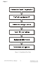
Appendix B. Block Diagram ........................................ 73
Appendix C. Screw-terminal Board............................. 75
C. 1 Introduction ................................................................................. 75
C. 2 Features ....................................................................................... 75
C. 3 Board Layout ............................................................................... 75
C.4 Pin Assignment ........................................................................... 76
C.5 Single-ended Connections........................................................... 77
C.6 Differential Connections .............................................................. 78
Appendix D. Register Structure and Format .............. 79
D.1 Overview...................................................................................... 79
D.2 I/O Port Address Map ................................................................. 79
D.3 A/D Single Value Acquisition — Write BASE+0 ......................... 83
D.4 Channel and A/D data — Read BASE + 0 ................................... 83
D.5 A/D Channel Range Setting — Write BASE+2 ............................ 84
D.6 MUX Control — Write BASE+4 .................................................. 85
D.7 A/D Control/Status Register — Write/Read BASE+6.................. 87
D.8 Clear interrupt and FIFO — Write BASE+8 ................................. 89
D. 9 Interrupt and FIFO status — Read BASE+8 ................................ 90
D.10 D/A control/status register — Write/Read BASE+A .................. 91
D.11 D/A Channel 0/1 Data — Write BASE+C/E ................................. 93
D.12 82C54 Counter Chip 0 — Write/Read BASE+10 to 16 .................. 94
D.13 82C54 counter chip 1 — Write/Read BASE+18 to 1E ................... 95