


– 83 –
APPENDIX D
PCI-1712/1712L User’s Manual
Advantech Co., Ltd.
www.advantech.com
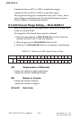
D.3 A/D Single Value Acquisition Write BASE+0
The A/D converter will convert one sample when you write to the
register Write BASE+0 with any value. User can check the A/D FIFO
status (A/D_F/E on register Read BASE+8) to make sure if the data is
ready to be received.
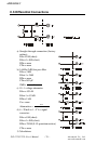
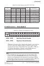
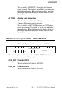
D.4 Channel and A/D data Read BASE + 0
These two bytes in Read BASE+0 hold the result of A/D conversion
data.
The 12 bits of data from the A/D conversion are stored in bit 0 to bit
11, bit 12 to 14 hold the A/D channel number and bit 15 holds the
trigger event flag.
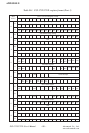
Table D-2: Register for channel number and A/D data
AD11 TO AD0 Data of A/D Conversion
AD0 the least significant bit (LSB) of A/D data.
AD11 the most significant bit (MSB) of A/D data.
CH2 to CH0 A/D Channel Number
CH2 ~ CH0 hold the A/D channel number from which the data is
received.
CH2 MSB.
CH0 LSB.
Note:
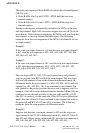
✎ A/D channel number specifies the channel from which data is derived.
CH2 is the MSB and CH0 is the LSB. For channel scan, there should
have 4 channel codes, specifically from CH0 to CH3. Because we have
not enough address space, bit 15 is used for other purposes instead for
CH3, which is hence not available..
AF A/D trigger event flag
The trigger flag indicates whether a trigger event has happened during
A/D conversion process.
.ddAesaB 51 41 31 21 11 01 9 8 7 6 5 4 3 2 1 0
0 R
atadD/AdnalennahC
FA 2HC 1HC 0HC 11DA 01DA 9DA 8DA 7DA 6DA 5DA 4DA 3DA 2DA 1DA 0DA