


183
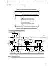
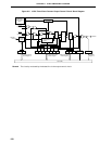
CHAPTER 8 16-BIT TIMER/EVENT COUNTER
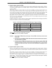
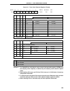
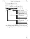
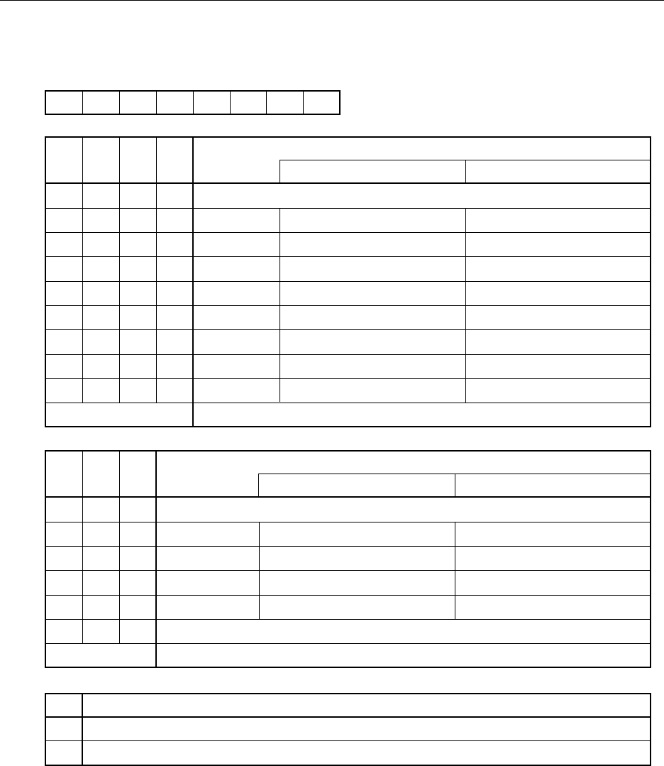
CLOE TCL06 TCL05 TCL04 TCL03 TCL02 TCL01 TCL00
<7>6543210Symbol
TCL0
TCL03 TCL02 TCL01 TCL00
0000f
XT
(32.768 kHz)
0101f
XX
f
X
(5.0 MHz) f
X
/2 (2.5 MHz)
0110f
XX
/2 f
X
/2
(2.5 MHz) f
X
/2
2
(1.25 MHz)
0111f
XX
/2
2
f
X
/2
2
(1.25 MHz) f
X
/2
3
(625 kHz)
1000f
XX
/2
3
f
X
/2
3
(625 kHz) f
X
/2
4
(313 kHz)
1001f
XX
/2
4
f
X
/2
4
(313 kHz) f
X
/2
5
(156 kHz)
1010f
XX
/2
5
f
X
/2
5
(156 kHz) f
X
/2
6
(78.1 kHz)
1011f
XX
/2
6
f
X
/2
6
(78.1 kHz) f
X
/2
7
(39.1 kHz)
1100f
XX
/2
7
f
X
/2
7
(39.1 kHz) f
X
/2
8
(19.5 kHz)
MCS = 1
PCL Output Clock Selection
MCS = 0
FF40H 00H R/W
Address After Reset R/W
Other than above Setting prohibited
TCL06 TCL05 TCL04
0 0 0 TI00 (Valid edge specifiable)
0012f
XX
Setting prohibited f
X
(5.0 MHz)
010f
XX
f
X
(5.0 MHz) f
X
/2 (2.5 MHz)
011f
XX
/2 f
X
/2 (2.5 MHz) f
X
/2
2
(1.25 MHz)
100f
XX
/2
2
f
X
/2
2
(1.25 MHz) f
X
/2
3
(625 kHz)
1 1 1 Watch timer output (INTTM 3)
MCS = 1
16-Bit Timer Register Count Clock Selection
MCS = 0
Other than above Setting prohibited
CLOE
1 Output enabled
PCL Output Control
0 Output disabled
Figure 8-3. Timer Clock Selection Register 0 Format
Cautions 1. The TI00/INTP0 pin valid edge is set by external interrupt mode register 0 (INTM0), and
the sampling clock frequency is selected by the sampling clock selection register
(SCS).
2. When enabling PCL output, set TCL00 to TCL03, then set 1 in CLOE with a 1-bit memory
manipulation instruction.
3. To read the count value when TI00 has been specified as the TM0 count clock, the value
should be read from TM0, not from 16-bit capture/compare register 01 (CR01).
4. When rewriting TCL0 to other data, stop the timer operation beforehand.