


325
CHAPTER 16 SERIAL INTERFACE CHANNEL 0 (
µ
PD78054 Subseries)
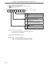
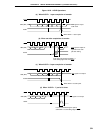
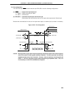
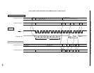
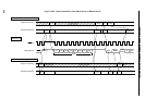
(5) Pin configuration
The serial clock pin SCK0 and serial data bus pin SB0 (SB1) have the following configurations.
(a) SCK0 ............ Serial clock input/output pin
<1> Master... CMOS and push-pull output
<2> Slave ..... Schmitt input
(b) SB0 (SB1) .... Serial data input/output dual-function pin
Both master and slave devices have an N-ch open drain output and a Schmitt input.
Because the serial data bus line has an N-ch open-drain output, an external pull-up resistor is necessary.
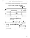
Figure 16-26. Pin Configuration
Caution Because the N-ch open-drain output must be high-impedance state at time of data reception,
write FFH to serial I/O shift register 0 (SIO0) in advance. The N-ch open-drain can be high-
impedance state at any time of transfer. However, when the wake-up function specify bit
(WUP) = 1, the N-ch open-drain output always becomes high-impedance state. Thus, it is
not necessary to write FFH to SIO0 before reception.
SI0
SO0
SI0
SO0
(Clock Input)
Clock Output
Master Device
Clock Input
(Clock Output)
Serial Clock
SCK0
SCK0
R
L
Serial Data Bus
SB0 (SB1) SB0 (SB1)
N-ch Open-Drain N-ch Open-Drain
Slave Device