


569
CHAPTER 27 INSTRUCTION SET
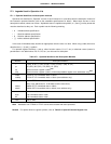
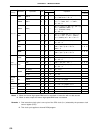
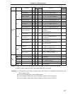
Clock Flag
Note 1 Note 2
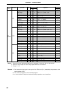
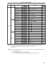
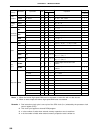
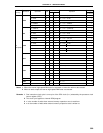
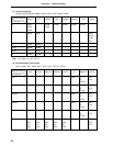
ZACCY
CY, saddr.bit 3 6 7 CY ← CY ∧ (saddr.bit) ×
CY, sfr.bit 3 – 7 CY ← CY ∧ sfr.bit ×
AND1 CY, A.bit 2 4 – CY ← CY ∧ A.bit ×
CY, PSW.bit 3 – 7 CY ← CY ∧ PSW.bit ×
CY, [HL].bit 2 6 7 + n CY ← CY ∧ (HL).bit ×
CY, saddr.bit 3 6 7 CY ← CY ∨ (saddr.bit) ×
CY, sfr.bit 3 – 7 CY ← CY ∨ sfr.bit ×
OR1 CY, A.bit 2 4 – CY ← CY ∨ A.bit ×
CY, PSW.bit 3 – 7 CY ← CY ∨ PSW.bit ×
CY, [HL].bit 2 6 7 + n CY ← CY ∨ (HL).bit ×
CY, saddr.bit 3 6 7 CY ← CY ∨ (saddr.bit) ×
CY, sfr.bit 3 – 7 CY ← CY ∨ sfr.bit ×
XOR1 CY, A.bit 2 4 – CY ← CY ∨ A.bit ×
CY, PSW. bit 3 – 7 CY ← CY ∨ PSW.bit ×
CY, [HL].bit 2 6 7 + n CY ← CY ∨ (HL).bit ×
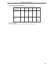
saddr.bit 2 4 6 (saddr.bit) ← 1
sfr.bit 3 – 8 sfr.bit ← 1
SET1 A.bit 2 4 – A.bit ← 1
PSW.bit 2 – 6 PSW.bit ← 1 ×××
[HL].bit 2 6
8 + n + m
(HL).bit ← 1
saddr.bit 2 4 6 (saddr.bit) ← 0
sfr.bit 3 – 8 sfr.bit ← 0
CLR1 A.bit 2 4 – A.bit ← 0
PSW.bit 2 – 6 PSW.bit ← 0 ×××
[HL].bit 2 6
8 + n + m
(HL).bit ← 0
SET1 CY 1 2 – CY ← 11
CLR1 CY 1 2 – CY ← 00
NOT1 CY 1 2 – CY ← CY ×
Notes 1. When the internal high-speed RAM area is accessed or instruction with no data access.
2. When an area except the internal high-speed RAM area is accessed.
Remarks 1. One instruction clock cycle is one cycle of the CPU clock (f
CPU) selected by the processor clock
control register (PCC).
2. This clock cycle applies to internal ROM program.
3. n is the number of waits when external memory expansion area is read from.
4. m is the number of waits when external memory expansion area is written to.
Mnemonic Operands Byte Operation
Instruction
Group
Bit
manipulate