


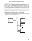

375
CHAPTER 17 SERIAL INTERFACE CHANNEL 0 (
µ
PD78054Y Subseries)
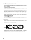
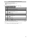
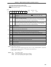
(c) Interrupt timing specification register (SINT)
SINT is set by the 1-bit or 8-bit memory manipulation instruction.
RESET input sets SINT to 00H.
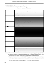
R/W WAT1 WAT0 Interrupt control by wait (See
Note 2
)
0 0 Interrupt service request is generated on rise of 8th SCK0 clock cycle (clock output is high
impedance).
0 1 Setting prohibited
1 0 Used in I
2
C bus mode (8-clock wait)
Generates an interrupt service request on rise of 8th SCL clock cycle. (In case of master device,
SCL pin is driven low after output of 8 clock cycles, to enter the wait state. In case of slave device,
SCL pin is driven low after input of 8 clock cycles, to require the wait state.)
1 1 Used in I
2
C bus mode (9-clock wait)
Generates an interrupt service request on rise of 9th SCL clock cycle. (In case of master device,
SCL pin is driven low after output of 9 clock cycles, to enter the wait state. In case of slave device,
SCL pin is driven low after input of 9 clock cycles, to require the wait state.)
R/W WREL Wait release control
0 Indicates that the wait state has been released.
1 Releases the wait state. Automatically cleared to 0 after releasing the wait state. This bit is used to release
the wait state set by means of WAT0 and WAT1.
R/W CLC Clock level control
0 Used in I
2
C bus mode. In cases other than serial transfer, SCL pin output is driven low.
1 Used in I
2
C bus mode. In cases other than serial transfer, SCL pin output is set to high impedance. (Clock
line is held high.) Used by master device to generate the start condition and stop condition signals.
R/W SVAM SVA bits used as slave address
0 Bits 0 to 7
1 Bits 1 to 7
R/W SIC INTCSAI0 interrupt source selection
Note 3
0 CSIIF0 is set to 1 after end of serial interface channel 0 transfer.
1 CSIIF0 is set to 1 after end of serial interface channel 0 transfer or when stop condition is detected.
R CLD SCL pin level (See
Note 4
)
0 Low level
1 High level
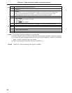
Notes 1. Bit 6 (CLD) is read-only.
2. When the I
2
C bus mode is used, be sure to set 1 and 0, or 1 and 1 in WAT0 and WAT1, respectively.
3. When using the wake-up function in I
2
C mode, be sure to set SIC to 1.
4. When CSIE0 = 0, CLD is 0.
Remark SVA : Slave address register
CSIIF0 : Interrupt request flag corresponding to INTCSI0
CSIE0 : Bit 7 of serial operating mode register 0 (CSIM0)
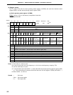
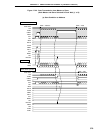
<6> <5> <4> <3> <2> 1 07
Symbol
SINT 0 CLD SIC
FF63H 00H R/W
Note1
Address After Reset R/W
SVAM CLC WREL
WAT1 WAT0