


267
CHAPTER 14 A/D CONVERTER
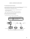
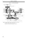
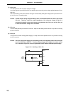
(1) Successive approximation register (SAR)
This register compares the analog input voltage value to the voltage tap (compare voltage) value applied from
the series resistor string and holds the result from the most significant bit (MSB).
When up to the least significant bit (LSB) is held (termination of A/D conversion), the SAR contents are
transferred to the A/D conversion result register (ADCR).
(2) A/D conversion result register (ADCR)
This register holds the A/D conversion result. Each time A/D conversion terminates, the conversion result
is loaded from the successive approximation register (SAR).
ADCR is read with an 8-bit memory manipulation instruction.
RESET input makes ADCR undefined.
(3) Sample & hold circuit
The sample & hold circuit samples each analog input signal sequentially applied from the input circuit and
sends it to the voltage comparator. This circuit holds the sampled analog input voltage value during A/D
conversion.
(4) Voltage comparator
The voltage comparator compares the analog input to the series resistor string output voltage.
(5) Series resistor string
The series resistor string is connected between AV
REF0 and AVSS and generates a voltage to be compared
to the analog input.
(6) ANI0 to ANI7 pins
These are 8-channel analog input pins to input analog signals to undergo A/D conversion to the A/D converter.
Pins other than those selected as analog input by the A/D converter input select register (ADIS) can be used
as input/output ports.
Cautions 1. Use ANI0 to ANI7 input voltages within the specified range. If a voltage higher than AV
REF0
or lower than AVSS is applied (even if within the absolute maximum ratings), the converted
value of the corresponding channel becomes indeterminate and may adversely affect the
converted values of other channels.
2. Analog input (ANI0 to ANI7) pins are multiplexed with the input/output port (port 1). When
performing A/D conversion with one of ANI0 to ANI7 selected, do not execute an input
instruction to port 1 during conversion. Otherwise, the conversion resolution may be
deteriorated. In addition, if a digital pulse is applied to a pin adjacent to the pin performing
A/D conversion, the desired A/D conversion value may not be obtained due to coupling
noise. Therefore, do not apply a pulse to a pin adjacent to the pin performing A/D
conversion.