


390
CHAPTER 17 SERIAL INTERFACE CHANNEL 0 (
µ
PD78054Y Subseries)
17.4.7 SCK0/SCL/P27 pin output manipulation
The SCK0/SCL/P27 pin can execute static output via software, in addition to outputting the normal serial clock.
The value of serial clocks can also be arbitrarily set by software (the SI0/SB0/SDA0 and SO0/SB1/SDA1 pins are
controlled with the RELT and CMDT bits of serial bus interface control register (SBIC)).
The SCK0/SCL/P27 pin output should be manipulated as described below.
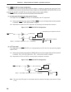
(1) In 3-wire serial I/O mode and 2-wire serial I/O mode
The output level of the SCK0/SCL/P27 pin is manipulated by the P27 output latch.
<1> Set the serial operating mode register 0 (CSIM0) (SCK0 pin is set in the output mode and serial operation
is enabled). SCK0 = 1 while serial transfer is stopped.
<2> Manipulate the content of the P27 output latch by executing the bit manipulation instruction.
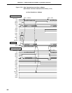
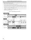
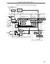
Figure 17-27. SCK0/SCL/P27 Pin Configuration
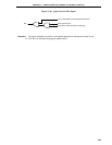
(2) In I
2
C bus mode
The output level of the SCK0/SCL/P27 pin is manipulated by the CLC bit of the interrupt timing specify
register (SINT).
<1> Set the serial operating mode register 0 (CSIM0) (SCL pin is set in the output mode and serial operation
is enabled). Set 1 to the P27 output latch. SCL = 0 while serial transfer is stopped.
<2> Manipulate the CLC bit of SINT by executing the bit manipulation instruction.
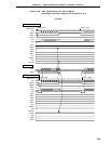
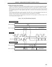
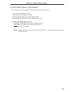
Figure 17-28. SCK0/SCL/P27 Pin Configuration
Note The level of the SCL signal is in accordance with the contents of the logic circuits shown in Figure
17-29.
SCK0/SCL/P27 To internal logic
P27
output latch
CSIE0 = 1 and CSIM01, CSIM00 are 1, 0 or 1, 1, respectively
SCK0 (1 while transfer is stopped)
From serial clock
controller
Manipulated by bit manipulation instruction
SCK0/SCL/P27 To internal logic
P27
output latch
CSIE0 = 1 and CSIM01 and CSIM00 are 1, 0 or 1, 1, respectively
SCL
Note
Set 1
From serial clock
controller