


293
CHAPTER 16 SERIAL INTERFACE CHANNEL 0 (
µ
PD78054 Subseries)
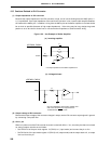
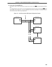
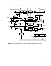
(3) SO0 latch
This latch holds SI0/SB0/P25 and SO0/SB1/P26 pin levels. It can be directly controlled also by software. In
the SBI mode, this latch is set upon termination of the 8th serial clock.
(4) Serial clock counter
This counter counts the serial clocks to be output and input during transmission/reception and to check whether
8-bit data has been transmitted/received.
(5) Serial clock control circuit
This circuit controls serial clock supply to the serial I/O shift register 0 (SIO0). When the internal system clock
is used, the circuit also controls clock output to the SCK0/P27 pin.
(6) Interrupt request signal generator
This circuit controls interrupt request signal generation. It generates the interrupt request signal in the following
cases.
• In the 3-wire serial I/O mode and 2-wire serial I/O mode
This circuit generates an interrupt request signal every eight serial clocks.
• In the SBI mode
When WUP is 0 ........... Generates an interrupt request signal every eight serial clocks.
When WUP is 1 ........... Generates an interrupt request signal when the serial I/O shift register 0 (SIO0)
value matches the slave address register (SVA) value after address reception.
Remark WUP is wake-up function specify bit. It is bit 5 of serial operating mode register 0 (CSIM0). To
use the wake-up function (WUP = 1), clear the bit 5 (SIC) of the interrupt timing specify register
(SINT) to 0.
(7) Busy/acknowledge output circuit and bus release/command/acknowledge detector
These two circuits output and detect various control signals in the SBI mode.
These do not operate in the 3-wire serial I/O mode and 2-wire serial I/O mode.