


70
CHAPTER 3 PIN FUNCTION (
µ
PD78054 Subseries)
3.2.13 AVDD
Analog power supply pin of A/D converter. Always use the same voltage as that of the V
DD
pin even when A/D
converter is not used.
3.2.14 AVSS
This is a ground voltage pin of A/D converter and D/A converter. Always use the same voltage as that of the VSS
pin even when neither A/D nor D/A converter is used.
3.2.15 RESET
This is a low-level active system reset input pin.
3.2.16 X1 and X2
Crystal resonator connect pins for main system clock oscillation. For external clock supply, input it to X1 and its
inverted signal to X2.
3.2.17 XT1 and XT2
Crystal resonator connect pins for subsystem clock oscillation.
For external clock supply, input it to XT1 and its inverted signal to XT2.
3.2.18 V
DD
Positive power supply pin
3.2.19 VSS
Ground potential pin
3.2.20 VPP (PROM versions only)
High-voltage apply pin for PROM programming mode setting and program write/verify. Directly connect to V
SS
in the normal operating mode.
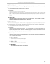
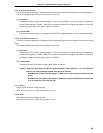
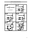
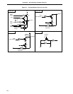
3.2.21 IC (Mask ROM version only)
The IC (Internally Connected) pin is provided to set the test mode to check the
µ
PD78054 Subseries before
shipment. Directly connect this pin to the VSS with the shortest possible wire in the normal operating mode.
When a voltage difference is produced between the IC pin and V
SS pin because the wiring between those two pins
is too long or an external noise is input to the IC pin, the user's program may not run normally.
Directly connect IC pins to VSS pins.
V
SS
IC
As short as possible