


Data exchange module 750-654
:$*2Ç,2 Ç6<67(0
5
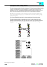
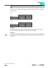
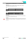
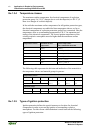
Structure of the in- and output data for CAL (from firmware WE)
Mode class 4:
The data is in the 2 Byte objects #BK_AI2W0_XXX, #BK_AI2W1_XXX and
#BK_A02W0_XXX. Each module has 2 values.
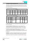
Input
Mux Content Description
n Input byte0, Input byte1 1. and 2. Input byte
n+1 Input byte2, Input byte3 3. and 4. Input byte
Output
Mux Content Description
n Output byte0, Output byte1 1. and 2. Output byte
n+1 Output byte2, Output byte3 3. and 4. Output byte
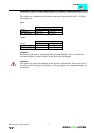
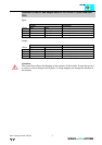
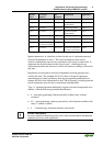
Mode class 0:
The description of the data is the same as for class 4 mode. The data is put into objects
No.1, No.2 and No.3 (read/write 2 Byte analog).
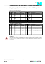
Attention:
The control byte allows the changing of the registers of the module. It must always be 0
in order to avoid a change in the registers. A wrong mapping can change the function of
the module!