


4–52 Cache and External Interfaces
21264/EV68A Hardware Reference Manual
Bcache Port
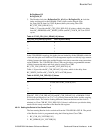
Table 4–45 lists the combination of control pin assertion for RAM_TYPE B.
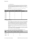
Table 4–46 lists the combination of control pin assertion for RAM_TYPE C.
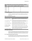
Table 4–47 lists the combination of control pin assertion for RAM_TYPE D.
Notes:
1. The NOP condition for RAM_TYPE B is consistent with bursting nonPentium
style SSRAMs.
2. In both
RAM_TYPE A and RAM_TYPE B, the pins BcDataOE_L and BcTagOE_L
function changes from output-enable control to chip-select control.
3. In both RAM_TYPE C and RAM_TYPE D SSRAMs, the pins
BcDataOE_L and
BcTagOE_L
function as an asynchronous output enable that envelopes the Bcache
read data by providing an extra cycle of output enable.
Using these Cbox CSRs, late-write nonbursting and dual-data rate SSRAMs can be
connected to the 21264/EV68A as described in Appendix E.
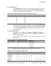
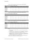
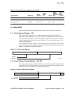
Table 4–45 Control Pin Assertion for RAM_TYPE B
TYPE_B NOP RA0 RA1 RA2 RA3 NOP NOP WA0 WA1 WA2 WA3 NOP
BcLoad_L HLHHHHHLHHHH
BcDataOE_L HLLLLHHLLLLH
BcDataWr_L LHHHHLLLLLLL
BcTagOE_L HLHHHHHLHHHH
BcTagWr_L HHHHHHHLHHHH
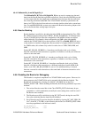
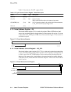
Table 4–46 Control Pin Assertion for RAM_TYPE C
TYPE_C NOP RA0 RA1 RA2 RA3 NOP NOP WA0 WA1 WA2 WA3 NOP
BcLoad_L HH H H H H HHHHHH
BcDataOE_L HH L L L L L HHHHH
BcDataWr_L HHHHH H HLLLLH
BcTagOE_L HL L H H H HHHHHH
BcTagWr_L HH H H H H HLHHHH
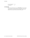
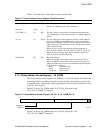
Table 4–47 Control Pin Assertion for RAM_TYPE D
TYPE_D NOP RA0 RA1 RA2 RA3 NOP NOP WA0 WA1 WA2 WA3 NOP
BcLoad_L HL HHHHHLHHHH
BcDataOE_L HHLL LL LHHHHH
BcDataWr_L HHHHHHHLLLLH
BcTagOE_L HHL LHHHHHHHH
BcTagWr_L HHHHHHHL HHHH