


21264/EV68A Hardware Reference Manual
Hardware Interface 3–3
21264/EV68A Signal Names and Functions
3.2 21264/EV68A Signal Names and Functions
Table 3–1 defines the 21264/EV68A signal types referred to in this section.
Table 3–2 lists all signal pins in alphabetic order and provides a full functional descrip-
tion of the pins. Table 3–4 lists the signal pins and their corresponding pin grid array
(PGA) locations in alphabetic order for the signal type. Table 3–5 lists the pin grid array
locations in alphabetical order.
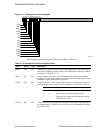
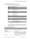
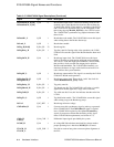
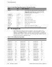
Table 3–1 Signal Pin Types Definitions
Signal Type Definition
Inputs
I_DC_REF Input DC reference pin
I_DA Input differential amplifier receiver
I_DA_CLK Input clock pin
Outputs
O_OD Open drain output driver
O_OD_TP Open drain driver for test pins
O_PP Push/pull output driver
O_PP_CLK Push/pull output clock driver
Bidirectional
B_DA_OD Bidirectional differential amplifier receiver with open drain output
B_DA_PP Bidirectional differential amplifier receiver with push/pull output
Other
Spare Reserved to COMPAQ
1
1
All Spare connections are Reserved to COMPAQ to maintain compatibility between
passes of the chip. Designers should not use these pins.
NoConnect No connection — Do not connect to these pins for any revision of the
21264/EV68A. These pins must float.
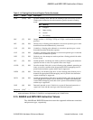
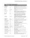
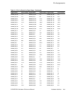
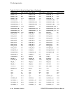
Table 3–2 21264/EV68A Signal Descriptions
Signal Type Count Description
BcAdd_H[23:4] O_PP 20 These signals provide the index to the Bcache.
BcCheck_H[15:0] B_DA_PP 16 ECC check bits for BcData_H[127:0].
BcData_H[127:0] B_DA_PP 128 Bcache data signals.
BcDataInClk_H[7:0] I_DA 8 Bcache data input clocks. These clocks are used with high
speed SDRAMs, such as DDRs, that provide a clock-out with
data-output pins to optimize Bcache read bandwidths. The
21264/EV68A internally synchronizes the data to its logic with
clock forward receive circuits similar to the system interface.
BcDataOE_L O_PP 1 Bcache data output enable. The 21264/EV68A asserts this sig-
nal during Bcache read operations.