


21264/EV68A Hardware Reference Manual
Electrical Data 9–7
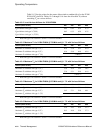
AC Characteristics
•
The AC specification values for TSU, TDH, and TSkew assume a ± 0.4 V input
signal amplitude, relative to Vref, one volt per nanosecond slew rates, no mismatch
in pin loading, and zero time-offset between forwarded clocks and data. Any devia-
tion from those conditions can result in degraded chip performance.
– VDD is in the range between 1.55 V and 1.65 V.
– SysVref is 1.2 Volts.
– BcVref is 0.75 Volts.
• All output skew data is based on simulation into a 50-ohm transmission line that is
terminated with 50 ohms to VDD/2 for Bcache timing, and with 50 ohms to VDD
for all other timing.
Timings are measured at the pins as follows:
– For open-drain outputs, timing is measured to (V
ol
+V
term
)/2. Where V
term
is
the offchip termination voltage for system signals.
– For non-open-drain outputs, timing is measured to (V
ol
+V
oh
)/2.
– For all inputs other than type I_DA_CLK, timing is measured to the point
where the input signal crosses VREF.
– For type I_DA_CLK inputs, timing is measured when the voltage on the com-
plementary inputs is equal.
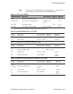
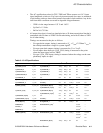
Table 9–13 AC Specifications
Signal Name Type Reference Signal TSU
1
TDH
2
TSkew Duty Cycle TSlew
SysAddIn_L[14:0 I_DA SysAddInClk_L 400 ps 400 ps NA NA 1.0 V/ns
SysFillValid_L I_DA SysAddInClk_L 400 ps 400 ps NA NA 1.0 V/ns
SysDataInValid_L I_DA SysAddInClk_L 400 ps 400 ps NA NA 1.0 V/ns
SysDataOutValid_L I_DA SysAddInClk_L 400 ps 400 ps NA NA 1.0 V/ns
SysAddInClk_L I_DA NA NA NA NA 45–55% 1.0 V/ns
SysAddOut_L[14:0] O_OD SysAddOutClk_L NA NA ± 300 ps
3
NA NA
SysAddOutClk_L O_OD EV6Clk_x NA NA ± 350 ps 45-55% NA
SysData_L[63:0] B_DA_OD SysDataInClk_H[7:0] 400 ps 400 ps NA NA 1.0 V/ns
SysDataOutClk_L[7:0]
4
NA NA ± 300 ps
3
NA NA
SysCheck_L[7:0] B_DA_OD SysDataInClk_H[7:0] 400 ps 400 ps NA NA 1.0 V/ns
SysDataOutClk_L[7:0]
4
NA NA ± 300 ps
3
NA NA
SysDataInClk_H[7:0] I_DA NA NA NA NA 45-55% 1.0 V/ns
SysDataOutClk_L[7:0] O_OD EV6Clk_x NA NA ± 350 ps 45-55% NA
BcAdd_H[23:4] O_PP BcTagOutClk_x NA NA ± 300 ps
5,6
NA —
BcDataOE_L O_PP BcDataOutClk_x[3:0]
7
45-55% —
BcLoad_L O_PP 38-63%
8
—
BcDataWr_L O_PP 40-60%
9
—
BcData_H[127:0] B_DA_PP BcDataOutClk_x[3:0]
10
NA NA ±300ps
6
45-55% 1.0 V/ns
38-63%
8
NA
40-60%
9
NA
BcDataInClk_H[7:0] 400 ps 400 ps NA NA NA