


21264/EV68A Hardware Reference Manual
Electrical Data 9–5
Power Supply Sequencing and Avoiding Potential Failure Mechanisms
9.3 Power Supply Sequencing and Avoiding Potential Failure Mech-
anisms
Before the power-on sequencing can occur, systems should ensure that DCOK_H is
deasserted and Reset_L is asserted. Then, systems ramp power to the 21264/EV68A
PLL_VDD @ 2.5 V and the 21264/EV68A power planes (VDD @ 1.65 V, not to
exceed 1.70 V under any circumstances), with PLL_VDD leading VDD. Systems
should supply differential clocks to the 21264/EV68A on ClkIn_H and ClkIn_L. The
clocks should be running as power is supplied.
When enabling the power supply inputs in a system, three failure mechanisms must be
avoided:
1. Bidirectional signal buses must not conflict during power-up. A conflict on these
buses can generate high current conditions, which can compromise the reliability of
the associated chips.
2. Similarly, input receivers should not see intermediate voltage levels that can also
generate high current conditions, which can compromise the reliability of the
receiving chip.
3. Finally, no CMOS chip should see an input voltage that is higher than its internal
VDD. In such a condition, a reasonable level of charge can be injected into the bulk
of the die. This condition can expose the chip to a positive-feedback latchup
condition.
The 21264/EV68A addresses those three failure mechanisms by disabling all of its
outputs and bidirectional pins (with three exceptions) until the assertion of DCOK_H.
The three exceptions are Tdo_H, EV6Clk_L,andEV6Clk_H. Tdo_H is used only in
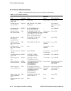
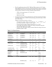
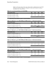
Table 9–11 Push-Pull Output Driver (O_PP)
Parameter
Symbol Description
Test
Conditions Minimum Maximum
V
OL
Low-level output voltage I
OL
= 40 mA — 500 mV
V
OH
High-level output voltage I
OL
= –40 mA VDD – 500 mV —
|I
OZ
| High-impedance output current 0 < V < VDD — 150 µA
C
OD
Open-drain pin capacitance Freq = 10 MHz — 6.0 pF
Note 6
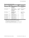
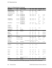
Table 9–12 Push-Pull Output Clock Driver (O_PP_CLK)
Parameter
Symbol Description
Test
Conditions Minimum Maximum
V
OL
Low-level output voltage Note 4 — VDD/2 – 325 mV
V
OH
High-level output voltage Note 4 VDD/2 + 325 mV —
|I
OZ
| High-impedance output
current
0 < V < VDD — 40 mA
1
1
Measured value includes current from onchip termination structures.