


21264/EV68A Hardware Reference Manual
Cache and External Interfaces 4–7
Bcache Structure
4.3 Bcache Structure
The 21264/EV68A Cbox provides control signals and an interface for a second-level
cache (Bcache).
The 21264/EV68A supports a Bcache from 1MB to 16MB, with 64-byte blocks. A 128-
bit bidirectional data bus is used for transfers between the 21264/EV68A and the
Bcache. The Bcache is fully synchronous and the synchronous static RAMs (SSRAMs)
must contain either one, two, or three internal registers. All Bcache control and address
pins are clocked synchronously on Bcache cycle boundaries. The Bcache clock rate
varies as a multiple of the CPU clock cycle in half-cycle increments from 1.5 to 4.0,
and in full-cycle increments of 5, 6, 7, and 8 times the CPU clock cycle. The 1.5 multi-
ple is only available in dual-data mode.
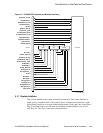
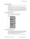
4.3.1 Bcache Interface Signals
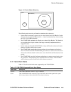
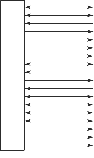
Figure 4–2 shows the 21264/EV68A system interface signals.
Figure 4–2 21264/EV68A Bcache Interface Signals
4.3.2 System Duplicate Tag Stores
The 21264/EV68A provides Bcache state support for systems with and without dupli-
cate tag stores, and will take different actions on this basis. The system sets the Cbox
CSR DUP_TAG_ENA[0], indicating that it has a duplicate tag store for the Bcache.
Systems using the DUP_TAG_ENA[0] bit must also use the Cbox CSR
BC_CLEAN_VICTIM[0] bit to avoid deadlock situations.
Systems using a Bcache duplicate tag store can accelerate system performance by:
21264
BcData_H[127:0]
FM-
05650
BcCheck_H[15:0]
BcDataInClk_H[7:0]
BcDataOutClk_x[3:0]
x
BcDataOE_L
BcDataWr_L
BcAdd_H[23:4]
BcTag_H[42:20]
BcTagInClk_H
BcTagOutClk_
x
BcVref
BcTagDirty_H
BcTagParity_H
BcTagShared_H
BcTagValid_H
BcTagOE_L
BcTagWr_L
BcLoad_L