


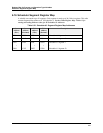

Register Map for Process and Operation Type Variables
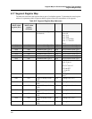
Device Control Group Register Map
76 HC900 Hybrid Controller Communications User Guide Revision 4
9/03
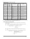
6.23 Device Control Group Register Map
Summary
This table contains addresses for the Device Control group #1.
See the Device Control Register Maps in Table 6-1 for starting and ending addresses (hex) for Device
Control Group #2 through Device Control Group #16 Map Addresses.
The Modbus Device Control number address for a Device Control can also be obtained from the Hybrid
Control Designer printout of "Block Modbus Addresses".
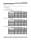
Function Code Support:
Reads – Function Code 3
Writes – Function Code 16 (10 hex) for preset of multiple registers (e.g., for floating point )
Writes – Function Code 6 for presetting an integer value
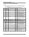
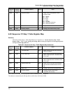
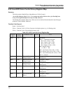
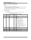
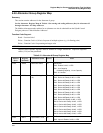
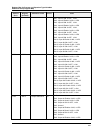
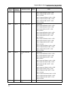
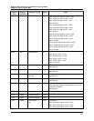
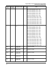
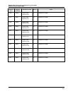
Table 6-30 Device Control #1 Group Register Map
Address
(hex)
Register
(decimal)
Parameter Name Access Notes
6B00 27393 Reset Request W Unsigned 16 Integer
Data Ignored
6B01 27394 Status Indicator R Bit Packed
Bits 0 – 6: Device Control State
Bit 0: Ready: 0=NO, 1=YES
Bit 1: Prestart: 0=NO, 1=YES
Bit 2: Starting: 0=NO, 1=YES
Bit 3: Running: 0=NO, 1=YES
Bit 4: Stopping: 0=NO, 1=YES
Bit 5: Disabled: 0=NO, 1=YES
Bit 6: Failed: 0=NO, 1=YES
Bit 7: Run Request Input State; 0=OFF, 1=ON
Bit 8: Device Feedback Started; 0=NO, 1=YES
Bit 9: Device Failed; 0=NO, 1=YES
Bit 10: Automatic Reset; 0=Manual, 1=Auto
Bit 11-15: Unused
6B02 27395 Remaining Delay
Time
R Floating Point in Seconds
6B04 27397 Start Delay R/W Floating Point in Seconds
6B06 27399 Stop Delay R/W Floating Point in Seconds
6B08 27401 Feedback Fail Delay R/W Floating Point in Seconds