14 Intel
®
31154 133 MHz PCI Bridge Design Guide Design Guide
Package Information
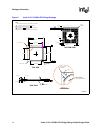
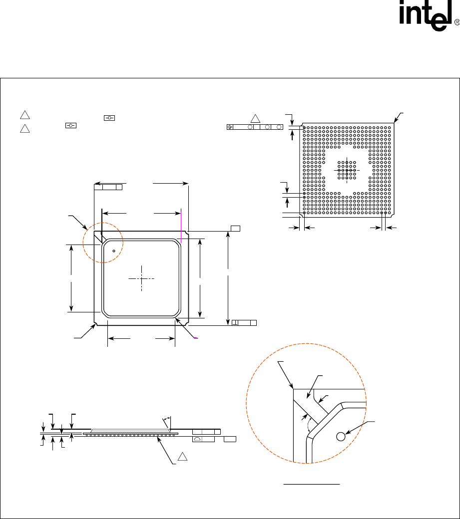
Figure 2. Intel
®
31154 133 MHz PCI Bridge Package
B1290-01
BOTTOM VIEW
SIDE VIEW
TOP VIEW
1.27
1
2
3
4
5
6
7
8
9
10
11
12
13
14
15
A
B
C
D
E
F
G
H
J
K
L
M
N
P
R
AA
Y
W
U
T
C
Ø
BA0.30
S
S S
Ø
1.53 REF 1.27
1.27
1.53 REF
PIN #1
CORNER
0.90
0.60
23
22
21
20
19
18
17
16
V
AB
AC
PIN #1 I.D. (SHINY)
1.0 DIA. X 0.15 DEPTH
9.0 X 9.0 FROM CENTER LINE
90.0˚
1.70
Au GATE
PIN #1 CORNER
NO RADIUS
SEE DETAIL "A"
45˚ CHAMFER
4 PLACES
(22.10 REF)
26.00 ± 0.20
(22.10 REF)
31.00 ± 0.10
31.00 ± 0.10
26.00 ± 0.20
3 X Ø1.00 THRU
0.61 ± 0.06
2.38 ± 0.21
30˚
0.60 ± 0.10
1.17 ± 0.05
SEATING PLANE
3
2
2
3
0.15
0.15
// C
0.127 A
-B-
0.127// A
-C-
NOT TO SCALE
DETAIL "A"
1. All dimensions and tolerances conform to ANSI Y14.5M-1982.
Dimension is measured at the maximum solder ball
diameter, parallel to primary datum
Primary datum and seating plane are defined by the
spherical crowns of the solder balls.
4. All dimensions, unless otherwise specified, are in millimeters.
Notes:


