


Intel
®
31154 133 MHz PCI Bridge Design Guide Design Guide 27
Terminations
§ §
NT_MASK#
• When forced retirement of the 31154 internal
request queues and data buffer is not desired
in the application, this pin must be pulled up to
3.3 V through an 8.2 KΩ resistor.
• When forced retirement of the 31154 internal
request queues and data buffer is desired in
the application, this pin must be connected to
external logic (or using the GPIO of the 31154)
that drives this pin low when masking new
transactions is desired.
• As soon as NT_MASK# is asserted, it must
not be de-asserted until the QE pin is
asserted.
• NT_MASK# must not be reasserted until the
QE pin is cleared.
• Setting the New Transaction Mask bit to 1b in
VCR0 has the same effect as asserting
NT_MASK#.
QE
Connection depends on application. This is an
output signal that indicates the state of the 31154
internal request and data queues. When high, this
signal indicates that the 31154 internal queues are
completely empty.
NOTE: The state of this output is valid only when
the NT_MASK# pin is asserted.
SCAN_EN For normal operation, tie low to GND.
TMODE[3:0]
For normal operation, tie to 0000 or 0111.
0 = Pull low to GND.
1 = Pull high to 3.3 V through an external 8.2 KΩ
resistor.
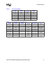
Table 5. Pull-Up/Pull-Down Terminations (Sheet 9 of 9)
Signal Pull-Up/Pull-Down or Termination (See Note 1) Comments
NOTES:
1. The recommended value for pull-up resistors for PCI applications is 5.6 KΩ (note that the minimum value for PCI 3.3 V
signaling R
MIN
= 2.42 KΩ, R
TYP
=8.2KΩ, as per the PCI Local Bus Specification, Revision 2.3, section 4.3.3).
2. The recommended value for pull-up resistors for PCI-X applications is 8.2 KΩ. For PCI-X, the minimum pull-up resistor value
is 5 KΩ, as per the PCI-X Addendum to the PCI Local Bus Specification, Revision 1.0b, section 9.7.
3. For plug-in card implementations, the pull-up must be on the motherboard.
4. Connect PVIO and SVIO pull-up resistors to 5 V or 3.3 V power supply through an external resistor—25 Ω (5 V) or
0 Ω (3.3 V), depending on the signaling level of the primary/secondary PCI bus. Refer to the power-sequencing guidelines in
Section 8.2 on page 58
.