Intel
®
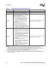
31154 133 MHz PCI Bridge Design Guide Design Guide 25
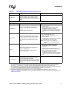
Terminations
JTAG
TCK Pull low when not used.
TDI
When not used, pull up to 3.3 V through an
external 8.2 KΩ resistor.
TDO NC when not used
TRST#
When not used, pull low to GND through an
external 1 KΩ resistor.
TMS
When not used, pull up to 3.3 V through an
external 8.2 KΩ resistor.
SCAN_EN For normal operation, tie low to GND.
TMODE[3:0]
For normal operation, tie to 0000 or 0111.
0 = Pull low to GND.
1 = Pull high to 3.3 V through an external 8.2 KΩ
resistor.
Voltages
S_VCCA
Connect to 1.3 V supply through a low-pass filter to
reduce noise-induced jitter. The 4.7 µF capacitor
must be low ESR solid tantalum, the 0.01 µF
capacitor must be of type X7R, and the node
connecting VCCPLL must be as short as possible.
• Ensure that the voltage at the input pin is
within the min./max. range for S_VCCA
(1.235 V and 1.365 V).
• For power sequencing, see Section 8.2,
“Power Sequencing” on page 58.
P_VCCA
Connect to 1.3 V supply through a low-pass filter to
reduce noise-induced jitter. The 4.7 µF capacitor
must be low ESR solid tantalum, the 0.01 µF
capacitor must be of type X7R, and the node
connecting VCCPLL must be as short as possible.
• Ensure that the voltage at the input pin is
within the min./max. range for P_VCCA
(1.235 V and 1.365 V).
• For power sequencing, see Section 8.2,
“Power Sequencing” on page 58.
VCC Connect to 1.3 V supply.
VCCP Connect to 3.3 V supply.
PVIO
Connect to 5 V or 3.3 V power supply through an
external resistor, depending on the signaling level
of primary PCI bus (see Note 4).
SVIO
Connect to 5 V or 3.3 V power supply through an
external resistor, depending on the signaling level
of secondary PCI bus (see Note 4).
Miscellaneous
R_REF
Pull down to GND through an external 30 Ω 1%
resistor.
MT0# and MT1#
Pull up to 3.3 V through an external 8.2 KΩ series
resistor.
Table 5. Pull-Up/Pull-Down Terminations (Sheet 7 of 9)
Signal Pull-Up/Pull-Down or Termination (See Note 1) Comments
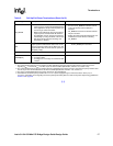
NOTES:
1. The recommended value for pull-up resistors for PCI applications is 5.6 KΩ (note that the minimum value for PCI 3.3 V
signaling R
MIN
= 2.42 KΩ, R
TYP
=8.2KΩ, as per the PCI Local Bus Specification, Revision 2.3, section 4.3.3).
2. The recommended value for pull-up resistors for PCI-X applications is 8.2 KΩ. For PCI-X, the minimum pull-up resistor value
is 5 KΩ, as per the PCI-X Addendum to the PCI Local Bus Specification, Revision 1.0b, section 9.7.
3. For plug-in card implementations, the pull-up must be on the motherboard.
4. Connect PVIO and SVIO pull-up resistors to 5 V or 3.3 V power supply through an external resistor—25 Ω (5 V) or
0 Ω (3.3 V), depending on the signaling level of the primary/secondary PCI bus. Refer to the power-sequencing guidelines in
Section 8.2 on page 58
.


