Intel
®
31154 133 MHz PCI Bridge Design Guide Design Guide 37
Routing Guidelines
6.2 EMI Considerations
It is highly recommended that you follow good EMI design practices when designing with the
31154:
• To minimize EMI on your PCB, a useful technique is not to extend the power planes to the
edge of the board.
• Another technique is to surround the perimeter of your PCB layers with a GND trace. This
helps to shield the PCB with grounds, minimizing radiation.
The AP-711 EMI Design Techniques Application Note discusses how to identify and prevent many
common EMI problems at the design stage. Although the document addresses a range of solutions,
emphasis is on printed circuit board design methods. This document is available at the following
link:
http://developer.intel.com/design/auto/mcs96/applnots/272673.htm
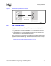
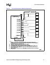
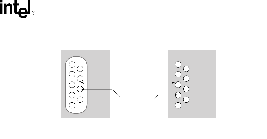
Figure 7. PCB Ground Layout Around Connectors
A9260-01
A. Incorrect method B. Correct method
Connector
GND PCB Layer
Connector Pins


