Intel
®
41210 Serial to Parallel PCI Bridge Developer’s Manual 49
Addressing
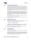
5.5.2 Prefetchable Memory Window
The prefetchable memory base and address registers, along with their upper 32-bit counterparts,
define an additional address range that the 41210 uses to forward accesses. Software maps the
prefetchable PCI memory spaces to this window. The 41210 still treats the memory reads in this
region as non-prefetchable. The 41210 forwards a memory transaction from PCI Express* to PCI
when the address falls within the range. The 41210 forwards transactions from PCI to PCI
Express* (or the peer PCI segment) when the address is outside the range and does not fall into the
regular memory range. This memory range supports 64-bit addressing, and has a granularity and
alignment of 1 MB.
The least-significant 32 bits of the range are defined by a 16-bit base register at offset 24h in the
configuration space and a 16-bit limit register at offset 28h. The most-significant 12 bits of each of
these registers correspond to bits[31:20] of the memory address. The least-significant 4 bits are
hard-wired to 1h, indicating 64-bit address support. The least-significant 20 bits of the base address
are assumed to be all 0s, which results in a natural alignment to a 1 MB boundary. The least-
significant 20 bits of the limit address are assumed to be all 1s, which results in an alignment to the
top of a 1 MB block.
The most-significant 32-bits of the range are defined by a 32-bit base register at offset 28h in the
configuration space, and a 32-bit limit register at offset 2Ch.
Note: Setting the entire base (with the most-significant 32-bits) to a value greater than that of the limit
turns off the memory range.
5.5.3 Opaque Memory Window
When the opaque memory window is enabled, the 41210 hard codes certain address ranges to the
secondary segment of each bridge.The hard-coded address ranges are as follows:
• A[63:62] = 10 Secondary side of A-Segment
• A[63:62] = 11 Secondary side of B-Segment
These address ranges are not forwarded from the PCI Express* interface to the corresponding
secondary side and are also never forwarded from the secondary to the PCI Express* interface,
regardless of the setting of the prefetchable base and limit registers.
Note: Even when the opaque memory window is enabled, the normal behavior defined for the BME,
MSE, and IOSE bits in the PCICMD register is still applicable.
5.6 VGA Addressing
When a VGA-compatible device exists behind a 41210 bridge, the VGA enable bit in the bridge
control register is set (offset 3 at 3Eh–3Fh).
When this bit is set, the 41210 forwards all transactions addressing the VGA frame buffer memory
and VGA I/O registers from PCI Express* to PCI, regardless of the values of the 41210 base and
limit address registers. When set, the 41210 does not forward VGA frame buffer memory accesses
to PCI Express* regardless of the values of the memory address ranges. However, the I/O enable
and memory enable bit in the command register must still be set.


