84 Intel
®
41210 Serial to Parallel PCI Bridge Developer’s Manual
Register Description
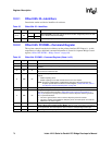
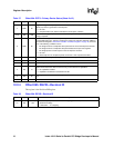
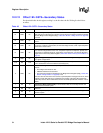
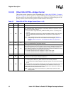
12.2.12 Offset 1Eh: SSTS—Secondary Status
For the writable bits in this register, writing 1 to the bit clears the bit. Writing 0 to the bit has
no effect.
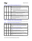
Table 46. Offset 1Eh: SSTS—Secondary Status
Bits Type Reset Description
15 RWC 0b
Detected Parity Error (DPE): This bit is set to 1 whenever the bridge detects an address or
data parity error on the PCI bus. This bit is set even when the Parity Error Response Enable
bit of the Bridge Control Register (bit[0], “Offset 3Eh: BCTRL—Bridge Control” on page 88)
is not set.
14 RWC 0b
Received System Error (RSE): This bit is set to 1 when a SERR# assertion is received
on PCI.
13 RWC 0b
Received Master Abort (RMA): This bit is set to 1 whenever the bridge, as an initiator on
the PCI bus, receives a master-abort, or when the bridge receives a PCI-X split completion
packet with a master-abort.
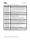
12 RWC 0b
Received Target Abort (RTA): This bit is set to 1 whenever the bridge, as an initiator on
PCI, receives a target-abort on PCI. For “completion required” PCI Express* packets, this
event forces a completion status of “target abort” on PCI Express*, and sets the Signaled
Target Abort in the Primary Status Register (“Offset 06h: PSTS—Primary Device Status” on
page 79).
11 RWC 0b
Signaled Target Abort (STA): This bit is set to 1 when the bridge, as a target on the PCI
bus, signals a target abort.
10:9 RO 01b
DEVSEL# Timing (DVT): These bits indicate that the 41210 responds in medium decode
time to transactions on the PCI interface (secondary bus).
8RWC 0b
Master Data Parity Error Detected (MDPD): This bit is set to 1 when all of the following
are true:
• The bridge is the initiator on PCI.
• PERR# is detected to be asserted.
• The Parity Error Response Enable bit in the Bridge Control Register (bit[0], “Offset 3Eh:
BCTRL—Bridge Control” on page 88) is set.
This bit is also set when the 41210 receives a split-completion message from PCI-X, which
indicates a write data parity error (regardless of the setting of the Parity Error Response
Enable bit). Refer to
PCI-X Addendum to the PCI Local Bus Specification, Revision 1.0b for
details.
7RO 1b
Fast Back-to-Back Capable (FBC): This bit indicates that the secondary interface can
receive fast back-to-back cycles.
6 RO 0b Reserved
5RO 1b
66 MHz Capable (C66): This bit indicates that the secondary interface of the bridge is
66 MHz-capable.
4:0 RO 00h Reserved


