Intel
®
41210 Serial to Parallel PCI Bridge Developer’s Manual 79
Register Description
12.2.3 Offset 06h: PSTS—Primary Device Status
For the writable bits in this register, writing a 1 clears the bit. Writing a 0 to the bit has no effect.
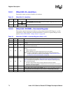
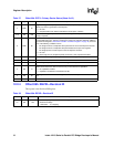
2RW 0b
Bus Master Enable (BME): This bit controls the ability of the 41210 to issue memory and
I/O read/write requests on the PCI Express* interface.
0 = The 41210 does not respond to any memory or I/O transactions on the PCI interface
and stops issuing new requests on PCI Express*.
1 = The 41210 processes transactions normally.
NOTE: This bit does not stop completions on PCI Express* from being issued. Software
must ensure that all upstream posted transactions are flushed in the bridge
segment when this bit is set. Otherwise, delayed completions (such as configuration
read completions) can be stuck behind a posted write and cannot proceed from PCI
to PCI Express*.
1RW 0b
Memory Space Enable (MSE): This bit controls the response of the 41210 when the 41210
is the target of a memory transaction from a primary or secondary interface.
0 = Every memory transaction targeting a secondary interface is master-aborted, and every
memory transaction from secondary to primary is claimed.
1 = Primary-to-secondary and secondary-to-primary forwarding follows the normal rules for
memory forwarding.
0RW 0b
I/O Space Enable (IOSE): This bit controls the response of the 41210 when the 41210 is
the target of I/O transactions from primary or secondary interfaces.
0 = Every I/O transaction targeting secondary is master-aborted, and every memory
transaction from secondary to primary is claimed, provided that the upstream I/O
enable bit in the BINIT register is also set.
1 = Primary-to-secondary and secondary-to-primary forwarding follows the normal rules for
memory forwarding.
Table 36. Offset 04h: PCICMD—Command Register (Sheet 2 of 2)
Bits Type Reset Description
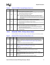
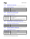
Table 37. Offset 06h: PSTS—Primary Device Status (Sheet 1 of 2)
Bits Type Reset Description
15 RWC 0b
Detected Parity Error (DPE): This bit is set when a poisoned TLP is received from PCI
Express* or a data parity error is detected from the peer PCI segment (writes or read
completions). This bit is set even when the parity error response enable bit (bit[6] of the
PCICMD Register—“Offset 04h: PCICMD—Command Register” on page 78) is not set.
0 = No error
1 = Poisoned TLP received or Data Parity Error detected
14 RWC 0b
Signaled System Error (SSE): This bit is set when ERR_FATAL or ERR_NONFATAL
messages are sent to the root complex and the SERR enable bit in the PCICMD Register
(“Offset 04h: PCICMD—Command Register” on page 78) is set.
0 = No error
1 = ERR_FATAL or ERR_NONFATAL message sent
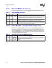
13 RWC 0b
Received Master Abort (RMA): This bit is set when the 41210 receives a completion with
“Unsupported Request Completion” status on the PCI Express* interface.
0 = No error
1 = “Unsupported Request Completion” status received on PCI Express* interface
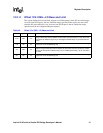
12 RWC 0b
Received Target Abort (RTA): This bit is set when the 41210 receives a completion with
“Completer Abort” (CA) status on the PCI Express* interface.
0 = No error
1 = Completer Abort (CA) status received on PCI Express* interface


