Intel
®
440GX AGPset Design Guide
2-13
Motherboard Layout and Routing Guidelines
Section 2.7, “Timing Analysis” on page 2-17 describes the timing analysis for the 100 MHz host
bus in more detail. Table 2-4 provides recommended flight time specifications for single and dual
Intel
®
Pentium
®
II processor systems. Flight times are measured at the Intel
®
Pentium
®
II
processor edge fingers. See the Pentium
®
II Processor Developer’s Manual
(order number 243502), Chapter 8, “GTL+ Interface Specifications“, for information on GTL+
timing measurements and signal quality specifications.
2.3.9 Topology Definition
GTL+ is sensitive to transmission line stubs, which can result in ringing on the rising edge caused
by the high impedance of the output buffer in the high state. GTL+ signals should be connected in a
daisy chain, keeping transmission line stubs to the Intel
®
440GX AGPset under 1.5 inches. Intel
®
Pentium
®
II processors should be placed at the end of the bus to properly terminate the GTL+
signals.
For a single Intel
®
Pentium
®
II processor design, Intel recommends that termination resistors be
placed at the other (AGPset) end of the bus. This provides the most robust signal integrity
characteristics and maximizes the range of trace lengths that will meet the flight time requirements.
The recommended termination resistor value is 56Ω ± 5%.
For dual Intel
®
Pentium
®
II processor based designs, a termination card must be placed in the
unused slot when only one processor is populated. This is necessary to ensure that signal integrity
requirements are met. Refer to Slot 1 Bus Termination Card Design Guidelines for details.
2.3.10 Pre-Layout Simulation (Sensitivity Analysis)
After an initial timing analysis has been completed, simulations should be performed to determine
the bounds on system layout. The layout recommendations in Section 4, “Debug
Recommendations” on page 4-1 are based on results of pre-layout simulations conducted by Intel.
GTL+ interconnect simulations using transmission line models are recommended to determine
signal quality and flight times for proposed layouts. Recommended parameter values can be
obtained if your supplier’s specific capabilities are known. The corner values should comprehend
the full range of manufacturing variation. Intel
®
Pentium
®
II processor models include the I/O
buffer models, core package parasitics, and substrate trace length, impedance and velocity. Intel
®
440GX AGPset models include the I/O buffers and package traces. Termination resistors should be
controlled to within ± 5%.
2.3.11 Simulation Methodolo
gy
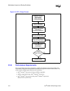
Pre-layout simulation allows the system “solution space” that meets flight time and signal quality
requirements to be understood before any routing is undertaken. Determining the layout
restrictions prior to physical design removes iteration cycles between layout and post layout
simulation, as shown in Figure 2-13.
Table 2-4. Recommended 100 MHz System Flight Time Specs
Driver Receiver T
flight,min
[ns] T
flight,max
[ns]
Intel
®
Pentium
®
II
processor
AGPset 0.36 2.13
Intel
®
440GX AGPset
Intel
®
Pentium
®
II
processor
0.37 1.76
Intel
®
Pentium
®
II
processor Intel
®
Pentium
®
II
processor
1.23 2.39


