Intel
®
440GX AGPset Design Guide
3-28
Design Checklist
3.14 System and Test Signals
•
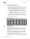
8.2K ohm pull-up resistor is recommended on the TEST# pin of the PIIX4E.
3.15 Power Management Signals
•
A power button is required by the ACPI specification.
•
PWRBTN# is connected to the front panel on/off power button. The PIIX4E integrates 16msec
debouncing logic on this pin.
•
All power button logic should be powered using 3VSB.
•
PS_POK from the ATX connector goes to AC power loss circuitry. This circuitry allows
control of whether the PIIX4E will power up after a power loss or remain off. The PIIX4E
defaults to powering up the system, which may cause system model implementation issues.
This circuit allows the user/BIOS to determine what will happen when a system is plugged in.
See
PIIX4E Application Note #7, System Power Control
, for details.
•
It is highly recommended that the PS_POK signal from the power supply connector not be
connected directly to logic on the board without first going through a Schmitt trigger input to
square-off and maintain its signal integrity.
•
PS_POK logic from the power supply connector can be powered from the core voltage supply.
•
RSMRST# logic should be powered by a standby supply, making sure that the input to the
PIIX4E is at a 3V level. The RSMST# signal requires a minimum time delay of 1 millisecond
from the rising edge of the standby power supply voltage. A Schmitt trigger circuit is
recommended to drive the RSMRST# signal. To provide the required rise time, the 1
millisecond delay should be placed before the Schmitt trigger circuit. The reference design
implements a 20ms delay at the input of the Schmitt trigger to ensure the Schmitt trigger
inverters have sufficiently powered up before switching the input. Also ensure that voltage on
RSMRST# does not exceed VCC(RTC). Refer to schematics for implementation details. If
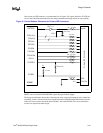
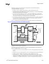
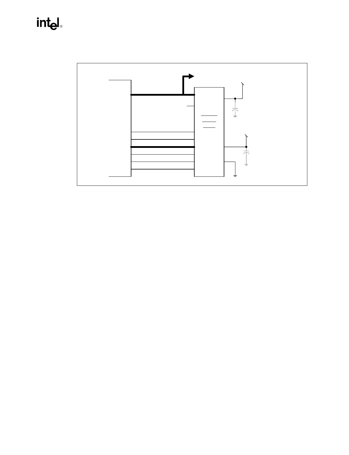
Figure 3-7. Interfacing Intel’s Flash with PIIX4E in Desktop
0.01uf
0.01 uf
SD
[
7:0
]
SUSA#
GPO
[
x
]
SD[7:0]
SA
[
17:0
]
MEMW#
MEMR#
BIOSCS#
Vpp
RP#
Vcc
WP#
Vcc
+5V
CE#
OE#
WE#
SA
[
17:0
]
2/4Mbit
BV/B5
Flash
BYTE#
DQ
[
7:0
]
DQ
[
14:8
]
N.C.
PIIX4
PIIX4E


