Intel
®
440GX AGPset Design Guide
3-25
Design Checklist
3.13 Flash Design
3.13.1 Dual-Footprint Flash Design
New features are coming to the PC continue to increase the size of BIOS code, pushing the limits
of the 1 Mbit boundary. OEMs have already converted many PC designs to 2 Mbit BIOS and
higher, and more will follow. Since it is difficult to predict when BIOS code will exceed 1 Mbit,
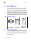
OEMs should design motherboards to be flexible. Design in a dual-footprint on the motherboard
that accepts both Intel’s 1 Mbit flash chips and 2 Mbit boot block chips. This will make the 1M-to-
2M transition easier by removing the need for PCB changes to accommodate higher density
components. Intel provides various layout tools to help OEMs design in the dual-footprint. These
tools are available from Intel’s BBS, WWW (http://www.intel.com/design/flcomp/devtools/
flas4.html), and literature distribution center. Look for Application Note AP-623 Multi-Site Layout
Planning with Intel's Boot Block Flash Memory (Order #: 292178). This document provides
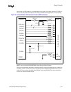
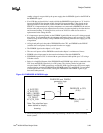
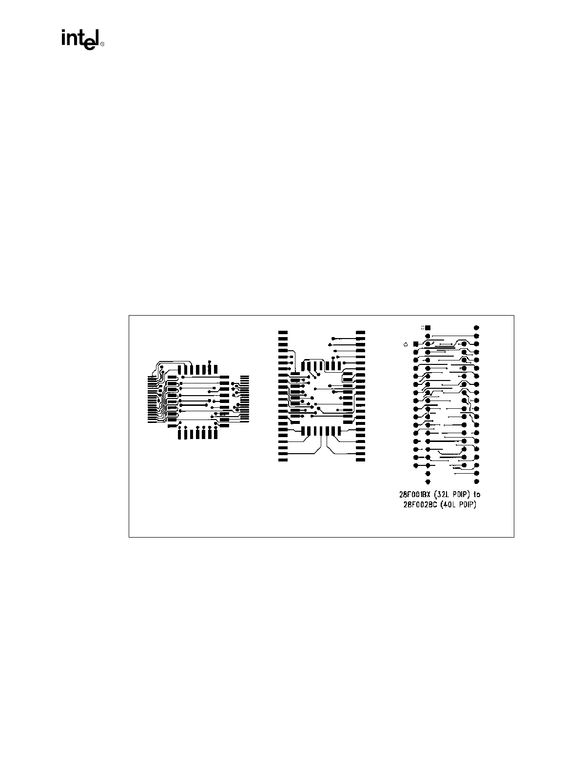
detailed information on flexible layouts. Shown below are three of the reference layouts that Intel
furnishes to customers. These layouts are described in AP-623 and are available electronically
(Gerber and Postscript formats). Note the small amount of extra board space needed to implement
the dual-footprint layouts.
3.13.2 Flash Design Considerations
The Intel’s flash devices (GX/BL/BV/B5) use an Address Transition Detection (ATD) mechanism
to improve their performance. When interfacing flash devices that employ the ATD mechanism, the
designer needs to make sure that the address transition time is not more than 10 ns while CE# is
active (low). If the address transition time is more than 10 ns invalid data can result on the data bus.
When flash devices are interfaced to the ISA bus they can be exposed to address transitions in
excess of 10 ns. Other types of interfacing considerations, specific to flash, can be referenced in
Application Note AP-636 “Preventing BIOS Failures Using Intel’s Boot Block Flash Memory”
(Order# 292192 or on WWW).
Figure 3-5. Dual Footprint Flash Layouts
PLCC32 to TSOP40 PLCC32 to PSOP44 PDIP32 to TDIP40


