Motherboard Layout and Routing Guidelines
2-22
Intel
®
440GX AGPset Design Guide
Some of the control signals require pull-up resistors to be installed on the motherboard. AGP
signals must be pulled up to VCC
3.3
using 8.2K to 10K ohm pull-up resistors (refer to
Section 3.5.1, “82443GX Interface” on page 3-10). Pull-up resistors should be discrete resistors, as
resistor packs will need longer stub lengths and may break timing. The stub to these pull-up
resistors needs to be controlled. The maximum stub length on a strobe trace is < 0.1 inch. The
maximum stub trace length on all other traces is < 0.5 inch.
Note: Under certain layouts, crosstalk and ground bounce can be observed on the AD_STB signals of the
AGP interface. Although Intel has not observed system failures due to this issue, we have improved
noise margin by enhancing the AGP buffers on the 82443GX. For new designs, additional margin
can be obtained by following these AGP layout guidelines.
2.9 82443GX Memory Subsystem Layout and Routing
Guidelines
2.9.1 100 MHz 82443GX Memory Array Considerations
Designing a reliable and high performance memory system will be challenging. Careful
consideration of motherboard routing and stackup topologies, DIMM topology, impedance, and
trace lengths must all be taken into account.
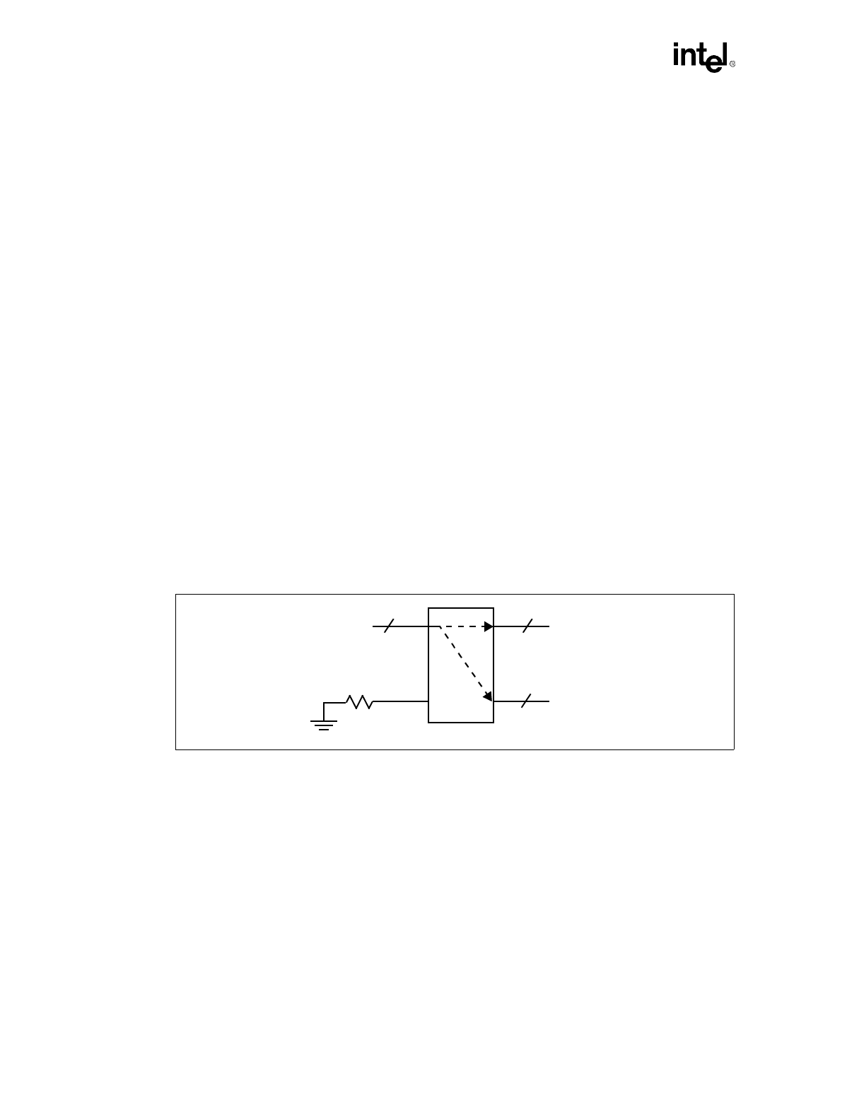
The 82443GX when configured with 4 double-sided DIMMs have heavy DQ loading. To offset the
heavy loading on the DQ lines, a FET switch mux is recommended to reduce the loading for
memory driving the 82443GX, and vice versa. An alternative NO-FET solution is also provided but
this solution has more strict routing restrictions.
To build large capacity DIMMs (i.e., 512 MB) using present day technology, x4 SDRAM devices
must be used. The loading on the control lines (MA/GXx, CS#, DQM, CK, etc.) are now twice the
loading of a x8 device. A DIMM which “registers” these control lines must be produced to meet
100 MHz timings (note that a PLL must be added to the registered DIMM and the additional PLL
jitter must be factored into the overall timing analysis). Electrical, thermal and layout topologies
for these registered DIMMs can be founded at the following Web address:
http://www.intel.com/design/pcisets/memory/index.htm
Figure 2-16. FET Switch Example
A2
to 82443GX MDs & MECCs
A1
B1
B2
to DIMM[1:0] DQs
to DIMM[3:2] DQs
