Intel
®
440GX AGPset Design Guide
3-24
Design Checklist
3.11 USB Interface
•
Contact your local Intel Field Sales representative for the following Application Note:
82371AB PIIX4 Application Note #1: USB Design Guide And Checklist Rev 1.1
. This
document discusses details of the PIIX4/PIIX4E implementation of the Universal Serial Bus.
Included in the discussion are motherboard layout guidelines, options for USB connector
implementation, USB clocking guidelines and a design checklist.
•
The AGP OVRCNT# pin should be pulled up with a 330K ohm resistor to 3.3V on the
motherboard to prevent this line from floating when there is no add-in card present.
3.12 IDE Interface
•
Support Cable Select(CSEL) is a PC97 requirement. The state of the cable select pin
determines the master/slave configuration of the hard drive at the end of the cable.
•
Primary IDE connector uses IRQ14 and the secondary IDE connector uses IRQ15.
•
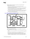
Layout - Proper operation of the IDE circuit depends on the total length of the IDE bus. The
total signal length from the IDE drivers to the end of the IDE cables should not exceed 18”.
Therefore, the PIIX4E should be located at close as possible to the ATA connectors to allow
the IDE cable to be as long as possible.
•
Use ISA reset signal RSTDRV from PIIX4E through a Schmitt trigger for RESET# signals.
•
IDEACTP# and IDEACTS# each need a 10K ohm (approximate) pull-up resistor to Vcc.
•
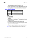
There is no internal pull-up or down on PDD7 or SDD7 of the PIIX4E. The ATA3
specification recommends a 10K ohm pull-down resistor on DD7. Devices shall not have a
pull-up resistor on DD7. It is recommended that a host have a 10K ohm pull-down resistor on
PDD7 and SDD7 to allow the host to recognize the absence of a device at power-up. This pull-
down resistor allows the BIOS to recognize the absence of an IDE slave device. Without this
pull-down, some BIOSs may take up to 30 seconds to recognize that there is no slave device,
or some BIOSs may hang the system.
•
If no IDE is implemented with the PIIX4E, the input signals (xDREQ and xIORDY) can be
grounded, and the output signals left as no connects. Unused ports can be tri-stated using the
General Configuration Register, address offset B0h–B3h, function 0.
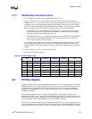
Table 3-12. Non-PIIX4E IDE
Pin Connection
Pin 28 of IDE connector (CSEL) 470 ohm pull-down.
Pin 19, 2, 22, 24, 26, 30, 40 of both ATA connectors Tie to Ground.
Pin 20, 32, 34of both ATA connectors Leave as a NC.


