Intel
®
440GX AGPset Design Guide
3-14
Design Checklist
3.6 Intel
®
440GX AGPset Memory Interface
3.6.1 SDRAM Connections
NOTES:
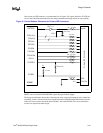
1. Some of the pin ranges above are dependent on which DIMM is being reviewed. “x” and “y” indicate signal
copies.
2. MAAxx address lines need to be routed to the two DIMM sockets closest to the 82443GX. MABxx# will be
routed to the one or two DIMM sockets furthest from the 82443GX. Selected MABxx# lines will also require
strapping options to properly configure the 82443GX.
3. Can either be a FET or no-FET solution. A FET solution will require the use of six 56-pin FET switch
multiplexers. The most common FET switches available are of the 5V family. A no-FET solution must adhere
to the strict no-FET design layout guidelines.
4. The MD, MECC and the DQM lines require “T” routing for load balancing.
5. Copies of SRAS#, SCAS#, WE# should be evenly distributed throughout the memory array.
6. MABxx# pins (except for MAB10, MAB13, and MAB14) are inverted for signal integrity reasons. MAB10,
MAB13, and MAB14 are not inverted to maintain correct SDRAM commands.
7. Series termination resistors are not required on the motherboard for DIMM signals (MD, MA, DQM, CS, etc.).
8. See the SDRAM Serial Presence Detect Data Structure specification for information on the EEPROM register
contents.
9. The
PC SDRAM Unbuffered DIMM Specification, Rev 1.0, dated Feb 1998
, shows pin 81 of the DIMM
module is the WP (write protect) pin for the SPD EEPROM. The block diagrams show there is a 47K pull-
down resistor tied to the WP pin. This allows the DIMM manufacturers to write SPD data to the EEPROM. An
OEM may wish to use the SPD EEPROM to write information into the DIMMs at production for system level
checkout to identify the DIMM installed as being shipped with the system. For this reason, the OEM may wish
to include some logic to control the level on pin 81 of the DIMM modules so that after the DIMM is tagged,
they can be write protected again. If this pin is pulled high on the motherboard, the DIMM SPD EEPROM is
write protected. Pin 81 of the DIMM sockets on the 82443GX dual processor reference schematics currently
shows a “NC”, no connects. If an OEM wishes to write protect the SDRAM SPD EEPROMS, then these pins
should be pulled high.
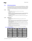
Table 3-6. SDRAM Connectivity
82443GX Pins/Connection DIMM Pins Pin Function
CKBF buffer outputs DCLK[x:y] CK[3:0] (4 DCLKs per DIMM) Clock
CS_A[7:0]# S#[1:0] (2 CS per DIMM) Chip Select
CS_B[7:0]# S#[3:2] (2 CS per DIMM) Chip Select
GND A13 Address
MAx[9:0]#, MAx10 A[10:0] Address
MAx11# BA0 Address
Max12# BA1 Address
MAA13#, MAB13 A11 Address
MAA14, MAB14 A12 Address
MDx[63:0] (from FET)
MD[63:0] (NO FET)
DQ[63:0] Data
MECC[7:0] CB[7:0] Error Checking and Correction
Strap for SMBus individual
Address
SA[2:0] SMBus Address
SMBDATA SDA SMBus Data
SMBCLK SCL SMBus Clock
SCASx# CAS# SDRAM Column Address Select
SRASx# RAS# SDRAM Row Address Select
WEx# WE0# Write Enable


