Intel
®
440GX AGPset Design Guide
2-15
Motherboard Layout and Routing Guidelines
2.5.1 Crosstalk and the Multi-Bit Adjustment Factor
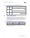
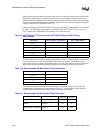
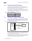
Coupled lines should be included in the post-layout simulations. The flight times listed in Table 2-4
apply to single bit simulations only. They include an allowance for crosstalk. Crosstalk effects are
accounted for, as part of the multi-bit timing adjustment factor, T
adj
, that is defined in Table 2-8.
The recommended timing budget includes 400 ps for the adjustment factor.
Use caution in applying T
adj
to coupled simulations. This adjustment factor encompasses other
effects besides board coupling, such as processor and package crosstalk, and ground return
inductances. In general, the additional delay introduced by coupled simulations should be less than
400 ps.
2.6 Validation
2.6.1 Flight Time Measurement
T
he timings for the Intel
®
Pentium
®
II processor are specified at the processor edge fingers. In
systems, the processor edges fingers are not readily accessible. In most cases, measurements must
be taken at the system board solder connection to the Slot 1 connector. To effectively correlate
delay measurements to values at the Pentium II processor edge fingers, the Slot 1 connector delay
must be incorporated.
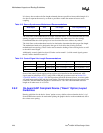
Flight time is defined as the difference between the delay of a signal at the input of a receiving
agent (measured at V
REF
), and the delay at the output pin of the driving agent when driving the
GTL+ reference load.
However, the driver delay into the reference load is not readily available, thus making flight time
measurement unfeasible. There are three options for dealing with this limitation:
•
The first option is to subtract the delay of the driver in the system environment (at the Slot 1
connection to the board) from the delay at the receiver. Such a measurement will introduce
uncertainty into the measurement due to differences between the driver delay in the reference
and system loads. If simulations indicate that your design has margin to the flight time
specifications, this approach will allow you to verify that the design is robust.
•
The second option is to subtract the simulated reference delay from the delay at the receiver.
The limitation of this option is that there may be 1 ns or more of uncertainty between the actual
driver delay and the results from a simulation. This approach is less accurate that the first
option.
•
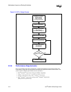
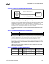
The final option is to simply use the measured delay from driver to receiver (T
measured
) to
validate that the system meets the setup and hold requirements. In this approach, the sum of
the driver delay and the flight time must fit within the “valid window” for setup and hold. The
timing requirements for satisfying the valid window are shown below.


