


6 - 20 6 - 20
MELSEC-Q
6 DATA COMMUNICATION USING THE NON PROCEDURE PROTOCOL
6.1.6 Received data count and receive complete code settings
The following default values have been set for the received data count and receive
complete code that are used for data reception with the non procedure protocol.
If it is necessary to change the following default settings, change the settings on the
GX Configurator-SC "Non procedure system setting" screen according to the
specifications of the external device (see Sections 8.4.5 and 8.4.7).
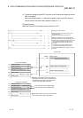
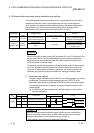
Setting data
Default
value
Allowable range
Buffer memory address where
the setting value is stored
Remarks
Received data
count
511 (1FF
H
)
Less than the size of the
receive data storage area
A4
H
/144
H
Unit is in accordance with the
word/byte units designation
0000
H
to 00FF
H
When any code is set
Receive
complete code
0D0A
H
(CR, LF)
FFFF
H
A5
H
/145
H
When there is no receive
complete code
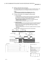
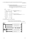
REMARK
Other than through the setting using GX Configurator-SC or the TO instruction at the
startup of the Q series C24, the received data count and receive complete code
setting values can be changed even after data communication has started if the
timing is as shown in the chart below.
The following describes the procedure for changing setting values for data reception
via the non procedure protocol after the start of data communication, and for the
resumption of data reception processing. Specifically, the module restrictions are
explained, along with the timing and procedure for changing the setting values.
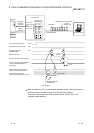
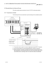
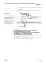
(1) Data receiving method
Reception using a dedicated instruction (INPUT) or an interrupt program ( 1) cannot
be performed. (Transmission using a dedicated instruction (OUTPUT) can be
performed.) Data must be received using the FROM instruction in the main program.
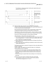
The following describes the I/O signals. (A program example is shown on the
following page.)
1 For details on the data reception using interrupt programs, see the User's
Manual (Application).
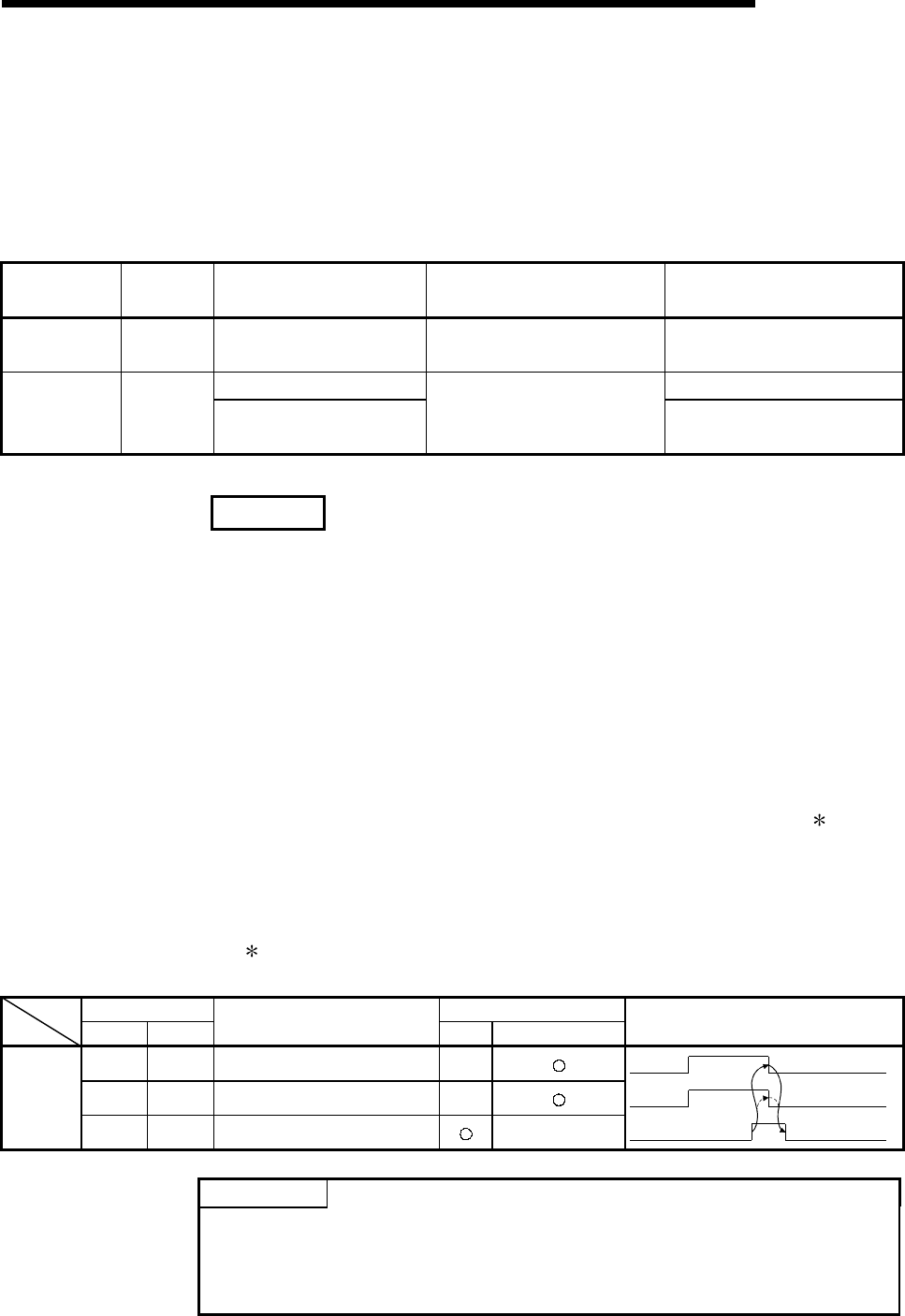
I/O signal Device that turns ON/OFF
CH1 side CH2 side
Signal name
CPU Q series C24
Timing
X3 XA
Reception data read request
X4 XB
Reception abnormal detection
Reception
Y1 Y8
Reception data read completion
(Only when normal)
(Only when abnormal)
POINT
When the reception abnormal detection signal (X4/XB) turns ON, read the error
code from the buffer memory below, and then check the type of error and take
corrective action based on the information found in Chapter 10.
• Data reception result storage area (addresses 258
H
/268
H
)