


Chapter 5 Signal Timing
DIO 6533 User Manual 5-28 © National Instruments Corporation
deasserting the ACK or REQ signal, respectively. Every clock cycle in
which both the ACK and REQ signals are high transfers one data point.
The 6533device can either drive an output clock signal onto the PCLK
line or receive an input clock signal from the PCLK line. By default, the
PCLK line is an input during output transfers, and an output during
input transfers. In the default configuration, because the clock direction
is the opposite of the data direction, any delay associated with the cable
between the 6533device and the peripheral device increases the data
hold time available, although decreasing the data setup time. If
necessary, for long cables, you can compensate for the decrease in data
setup time by slowing down the PCLK clock.
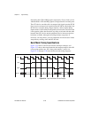
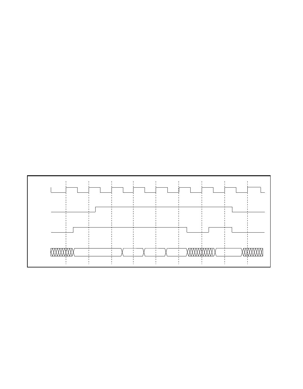
Burst Mode Timing Specifications
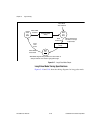
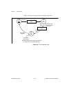
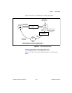
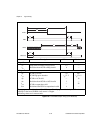
Figure5-24 shows a burst mode transfer data input example, and
Figure5-25 shows a burst mode transfer data output example, where D1
is data point number one, D2 is data point number2, and so on.
Figures5-26 through5-29 show the burst mode timing diagrams.
Figure 5-24.
Input Burst Mode Transfer Example
PCLK
ACK
Data In
REQ
D5
D1
D2 D3 D4