Rev.2.00 Nov 28, 2005 page 220 of 378
REJ09B0124-0200
M16C/6N Group (M16C/6NK, M16C/6NM) 17. D/A Converter
Under development
This document is under development and its contents are subject to change.
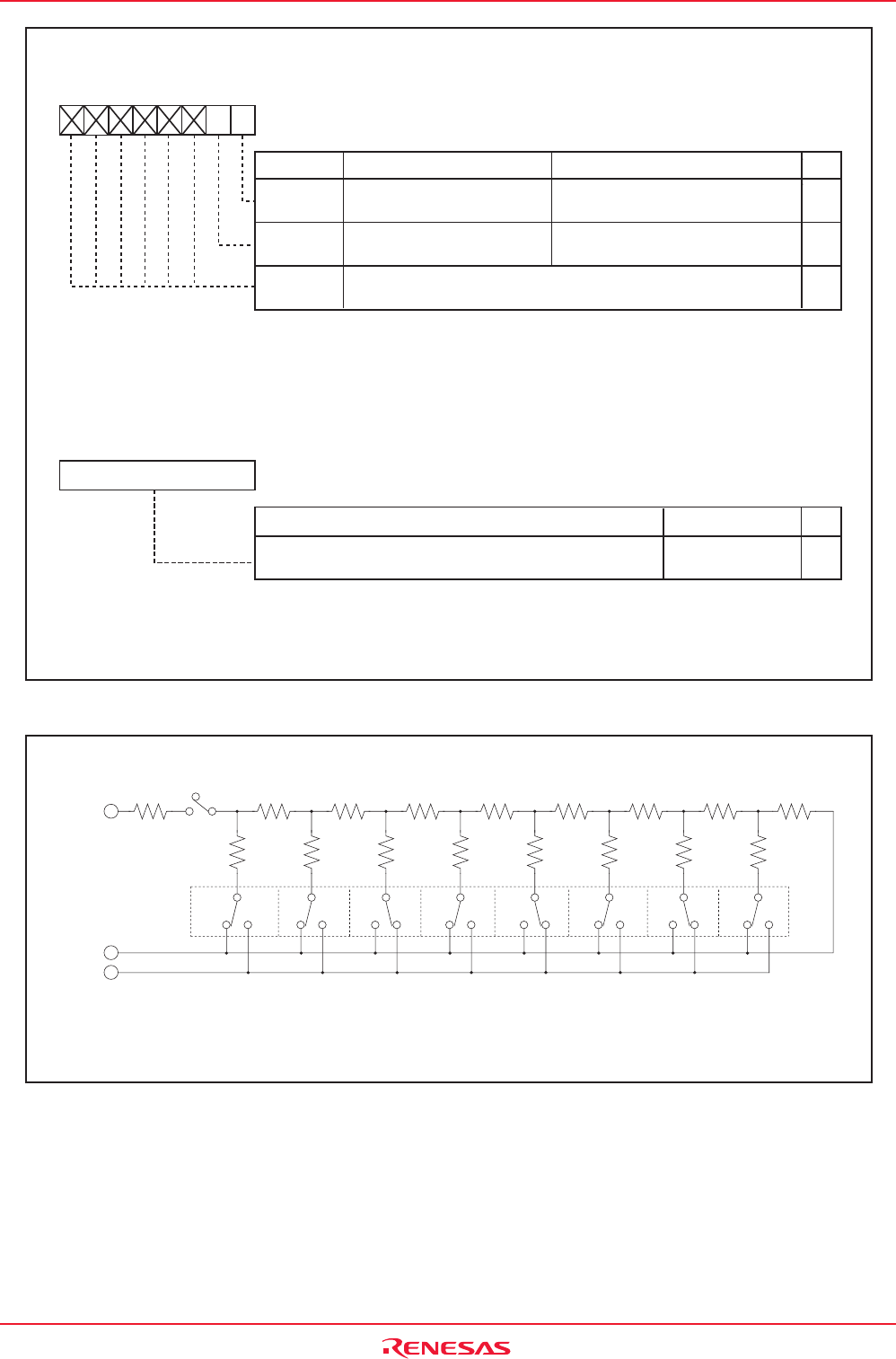
Figure 17.2 DACON Register, DA0 and DA1 Registers
Figure 17.3 D/A Converter Equivalent Circuit
D/A Control Register
(1)
Symbol Address After Reset
Symbol Address After Reset
DACON 03DCh
03D8h
03DAh
00h
b7 b6 b5 b4 b3 b2 b1 b0
D/A0 Output Enable Bit
Bit Symbol Bit Name Function
RW
D/A1 Output Enable Bit
DA0
DA1
00h
00h
b7 b0
Function
Output value of D/A conversion
RW
RW
-
RW
RW
DA0E
DA1E
-
(b7-b2)
0 : Output disabled
1 : Output enabled
0 : Output disabled
1 : Output enabled
Nothing is assigned. When write, set to "0".
When read, their contents are "0".
NOTE:
1. When not using the D/A converter, set the DAiE bit (i = 0, 1) to "0" (output disabled) to reduce the unnecessary
current consumption in the chip and set the DAi register to "00h" to prevent current from flowing into the R-2R
resistor ladder.
NOTE:
1. When not using the D/A converter, set the DAiE bit (i = 0, 1) to "0" (output disabled) to reduce the unnecessary
current consumption in the chip and set the DAi register to "00h" to prevent current from flowing into the R-2R
resistor ladder.
D/A Register i (i = 0, 1)
(1)
00h to FFh
Setting Range
2R
R
2R
R
2R
R
2R
R
2R
R
2R
R
2R
R
2R
2R
DAiE bit
"1""0"
MSB LSB
DAi register
r
i = 0, 1
NOTES:
1. The above diagram shows an instance in which the DAi register is assigned "2Ah".
2. VREF is not related to VCUT bit setting in the ADCON1 register.
"1"
"0"
VREF
(2)
AVSS
DAi


