Rev.2.00 Nov 28, 2005 page 63 of 378
REJ09B0124-0200
M16C/6N Group (M16C/6NK, M16C/6NM) 8. Clock Generating Circuit
Under development
This document is under development and its contents are subject to change.
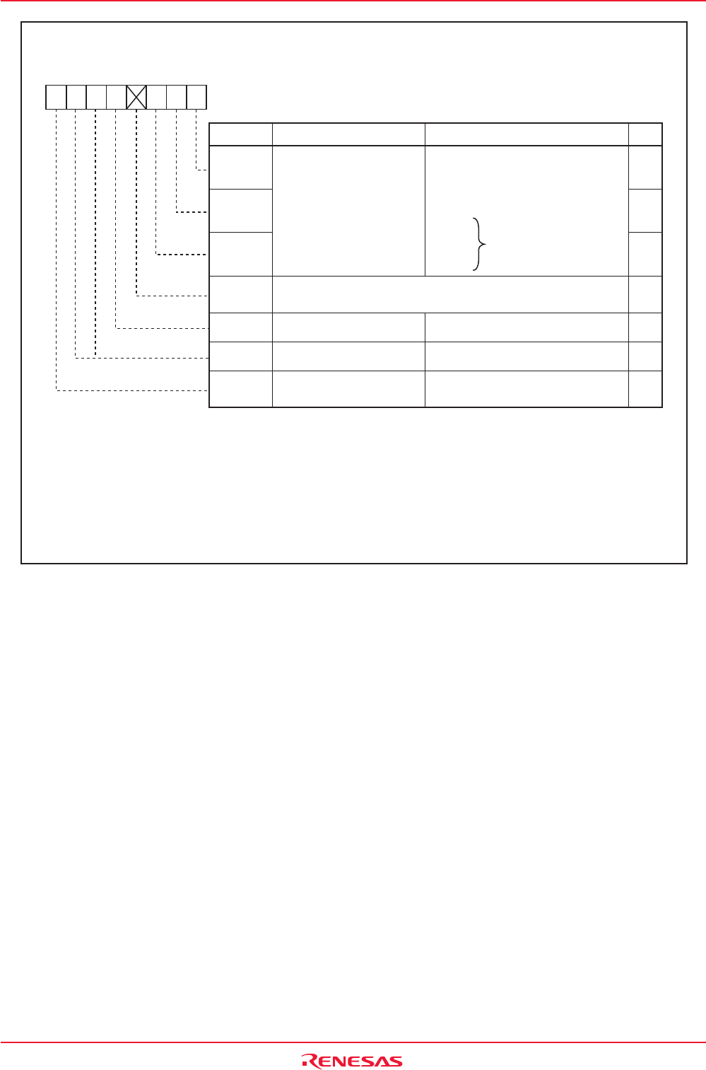
Figure 8.8 PLC0 Register
PLC07
Function
PLL Control Register 0
(1)
Operation Enable Bit
(3)
0 : PLL Off
1 : PLL On
Bit NameBit Symbol
Symbol Address After Reset
PLC0 001Ch 0001X010b
RW
PLC00
b2 b1 b0
0 0 0 : Do not set a value
0 0 1 : Multiply by 2
0 1 0 : Multiply by 4
0 1 1 : Multiply by 6
(4)
1 0 0 :
1 0 1 :
Do not set a value
1 1 0 :
1 1 1 :
PLC01
PLC02
-
(b3)
-
(b4)
-
(b6-b5)
Reserved Bit Set to "1"
Reserved Bit Set to "0"
PLL Multiplying Factor
Select Bit
(2)
RW
RW
RW
-
RW
RW
RW
Nothing is assigned. When write, set to "0".
When read, its content is indeterminate.
NOTES:
1. Write to this register after setting the PRC0 bit in the PRCR register to "1" (write enable).
2. This bit can only be modified when the PLC07 bit = 0 (PLL turned off). The value once written to this bit
cannot be modified.
3. Before setting this bit to "1", set the CM07 bit in the CM0 register to "0" (main clock), set the CM17 to
CM16 bits in the CM1 register to "00b" (main clock undivided mode), and set the CM06 bit in the CM0
register to "0" (CM16 and CM17 bits enable).
4. Multiply by 6 is available Normal-ver. only.
b7 b6 b5 b4 b3 b2 b1 b0
0 10


