Rev.2.00 Nov 28, 2005 page 306 of 378
REJ09B0124-0200
M16C/6N Group (M16C/6NK, M16C/6NM) 22. Electric Characteristics (Normal-ver.)
Under development
This document is under development and its contents are subject to change.
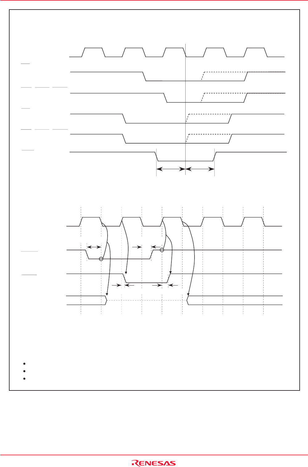
Figure 22.5 Timing Diagram (2)
Measuring conditions :
VCC = 5 V
Input timing voltage : Determined with V
IL
= 1.0 V, V
IH
= 4.0 V
Output timing voltage: Determined with V
OL
= 2.5 V, V
OH
= 2.5 V
BCLK
HOLD input
HLDA output
P0, P1, P2,
P3, P4,
P5_0 to P5_2
(1)
NOTE:
1.
The above pins are set to high-impedance regardless of the input level of the BYTE pin,
the PM06 bit in the PM0 register and the PM11 bit in the PM1 register.
Hi—Z
RDY input
BCLK
RD
(Multiplexed bus)
(Multiplexed bus)
WR, WRL, WRH
WR, WRL, WRH
(Separate bus)
RD
(Separate bus)
t
d(BCLK—HLDA)
t
d(BCLK—HLDA)
t
h(BCLK—HOLD)
t
su(HOLD—BCLK)
tsu(RDY—BCLK) th(BCLK—RDY)
Memory Expansion Mode and Microprocessor Mode
(Effective for setting with wait)
(Common to setting with wait and setting without wait)
VCC = 5V


