


TMS320C6712D
FLOATINGĆPOINT DIGITAL SIGNAL PROCESSOR
SPRS293A − OCTOBER 2005 − REVISED NOVEMBER 2005
29
POST OFFICE BOX 1443 • HOUSTON, TEXAS 77251−1443
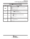
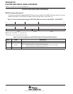
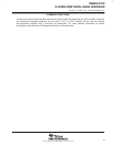
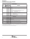
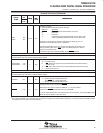
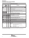
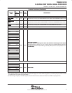
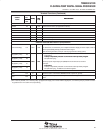
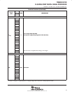
Terminal Functions (Continued)
SIGNAL
PIN
NO.
TYPE
†
IPD/
‡
DESCRIPTION
SIGNAL
NAME
GDP/
ZDP
TYPE
†
IPD/
IPU
‡
DESCRIPTION
MULTICHANNEL BUFFERED SERIAL PORT 0 (McBSP0)
CLKS0 K3 I IPD External clock source (as opposed to internal)
CLKR0 H3 I/O/Z IPD Receive clock
CLKX0 G3 I/O/Z IPD Transmit clock
DR0 J1 I IPU Receive data
DX0 H2 O/Z IPU Transmit data
FSR0 J3 I/O/Z IPD Receive frame sync
FSX0 H1 I/O/Z IPD Transmit frame sync
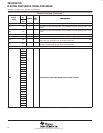
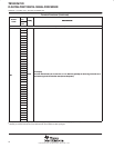
GENERAL-PURPOSE INPUT/OUTPUT (GPIO) MODULE
CLKOUT2/GP[2] Y12 I/O/Z IPD
Clock output at half of device speed
For this device, the CLKOUT2 pin is multiplexed with the GP[2] pin. Clock output at half of
device speed (O/Z) [default] (SYSCLK2 internal signal
from the clock generator) or this pin can be programmed as GP[2] (I/O/Z).
GP[7](EXT_INT7) E3
External interrupts
• Edge-driven
Polarity independently selected via the External Interrupt Polarity Register
GP[6](EXT_INT6) D2
I/O/Z
IPU
Edge-driven
• Polarity independently selected via the External Interrupt Polarity Register
bits (EXTPOL.[3:0])
GP[5](EXT_INT5) C1
I/O/Z IPU
General-purpose input/output pins (I/O/Z) which also function as external
interrupts
• Edge-driven
GP[4](EXT_INT4) C2
•
Edge-driven
• Polarity independently selected via the External Interrupt Polarity Register
bits (EXTPOL.[3:0]), in addition to the GPIO registers.
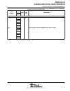
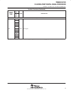
RESERVED FOR TEST
RSV C12 O − Reserved (leave unconnected, do not connect to power or ground)
RSV D12 I −
For proper device operation, the D12 pin must be externally pulled down with a 10-kΩ re-
sistor.
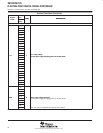
†
I = Input, O = Output, Z = High impedance, S = Supply voltage, GND = Ground, A = Analog signal (PLL Filter)
‡
IPD = Internal pulldown, IPU = Internal pullup. [To oppose the supply rail on these IPD/IPU signal pins, use external pullup or pulldown resistors
no greater than 4.4 kΩ and 2.0 kΩ, respectively.]