


TMS320C6712D
FLOATINGĆPOINT DIGITAL SIGNAL PROCESSOR
SPRS293 − OCTOBER 2005
87
POST OFFICE BOX 1443 • HOUSTON, TEXAS 77251−1443
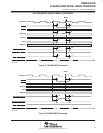
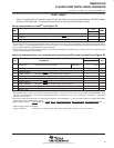
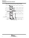
MULTICHANNEL BUFFERED SERIAL PORT TIMING
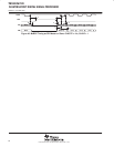
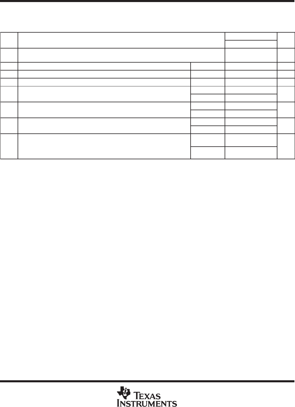
switching characteristics over recommended operating conditions for McBSP
†‡
(see Figure 41)
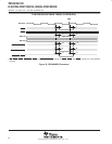
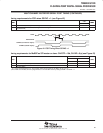
NO.
PARAMETER
−150
UNIT
NO.
PARAMETER
MIN MAX
UNIT
1 t
d(CKSH-CKRXH)
Delay time, CLKS high to CLKR/X high for internal CLKR/X generated from
CLKS input
1.8 10 ns
2 t
c(CKRX)
Cycle time, CLKR/X CLKR/X int 2P
§¶
ns
3 t
w(CKRX)
Pulse duration, CLKR/X high or CLKR/X low CLKR/X int C − 1
#
C + 1
#
ns
4 t
d(CKRH-FRV)
Delay time, CLKR high to internal FSR valid CLKR int −2 3 ns
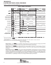
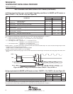
9
t
d(CKXH-FXV)
Delay time, CLKX high to internal FSX valid
CLKX int −2 3
ns
9 t
d(CKXH-FXV)
Delay time, CLKX high to internal FSX valid
CLKX ext
2 9
ns
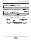
12
t
dis(CKXH-DXHZ)
Disable time, DX high impedance following last data bit from
CLKX int −1 4
ns
12 t
dis(CKXH-DXHZ
)
Disable time, DX high impedance following last data bit from
CLKX high
CLKX ext
1.5 10
ns
13
t
d(CKXH-DXV)
Delay time, CLKX high to DX valid
CLKX int −3.2 + D1
||
4 + D2
||
ns
13 t
d(CKXH-DXV)
Delay time, CLKX high to DX valid
CLKX ext
0.5 + D1
||
10+ D2
||
ns
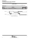
14
t
d(FXH-DXV)
Delay time, FSX high to DX valid
FSX int −1 7.5
ns
14 t
d(FXH-DXV)
ONLY applies when in data
delay 0 (XDATDLY = 00b) mode
FSX ext 2 11.5
ns
†
CLKRP = CLKXP = FSRP = FSXP = 0. If polarity of any of the signals is inverted, then the timing references of that signal are also inverted.
‡
Minimum delay times also represent minimum output hold times.
§
P = 1/CPU clock frequency in ns. For example, when running parts at 150 MHz, use P = 6.7 ns.
¶
The minimum CLKR/X period is twice the CPU cycle time (2P) and not faster than 75 Mbps (13.3 ns). This means that the maximum bit rate for
communications between the McBSP and other device is 75 Mbps for 150 MHz CPU clock; where the McBSP is either the master or the slave.
Care must be taken to ensure that the AC timings specified in this data sheet are met. The maximum bit rate for McBSP-to-McBSP
communications is 67 Mbps; therefore, the minimum CLKR/X clock cycle is either twice the CPU cycle time (2P), or 15 ns (67 MHz), whichever
value is larger. For example, when running parts at 150 MHz (P = 6.7 ns), use 15 ns as the minimum CLKR/X clock cycle (by setting the
appropriate CLKGDV ratio or external clock source). When running parts at 60 MHz (P = 16.67 ns), use 2P = 33 ns (30 MHz) as the minimum
CLKR/X clock cycle. The maximum bit rate for McBSP-to-McBSP communications applies when the serial port is a master of the clock and frame
syncs (with CLKR connected to CLKX, FSR connected to FSX, CLKXM = FSXM = 1, and CLKRM = FSRM = 0) in data delay 1 or 2 mode
(R/XDATDLY = 01b or 10b) and the other device the McBSP communicates to is a slave.
#
C = H or L
S = sample rate generator input clock = 2P if CLKSM = 1 (P = 1/CPU clock frequency)
= sample rate generator input clock = P_clks if CLKSM = 0 (P_clks = CLKS period)
H = CLKX high pulse width = (CLKGDV/2 + 1) * S if CLKGDV is even
= (CLKGDV + 1)/2 * S if CLKGDV is odd or zero
L = CLKX low pulse width = (CLKGDV/2) * S if CLKGDV is even
= (CLKGDV + 1)/2 * S if CLKGDV is odd or zero
CLKGDV should be set appropriately to ensure the McBSP bit rate does not exceed the maximum limit (see ¶ footnote above).
||
Extra delay from CLKX high to DX valid applies only to the first data bit of a device, if and only if DXENA = 1 in SPCR.
If DXENA = 0, then D1 = D2 = 0
If DXENA = 1, then D1 = 2P, D2 = 4P