


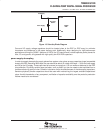
TMS320C6712D
FLOATINGĆPOINT DIGITAL SIGNAL PROCESSOR
SPRS293A − OCTOBER 2005 − REVISED NOVEMBER 2005
53
POST OFFICE BOX 1443 • HOUSTON, TEXAS 77251−1443
general-purpose input/output (GPIO)
To use the GP[7:4, 2] software-configurable GPIO pins, the GPxEN bits in the GP Enable (GPEN) Register and
the GPxDIR bits in the GP Direction (GPDIR) Register must be properly configured.
GPxEN = 1 GP[x] pin is enabled
GPxDIR = 0 GP[x] pin is an input
GPxDIR = 1 GP[x] pin is an output
where “x” represents one of the 7 through 4, or 2 GPIO pins
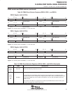
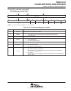
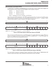
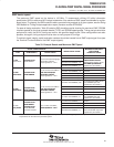
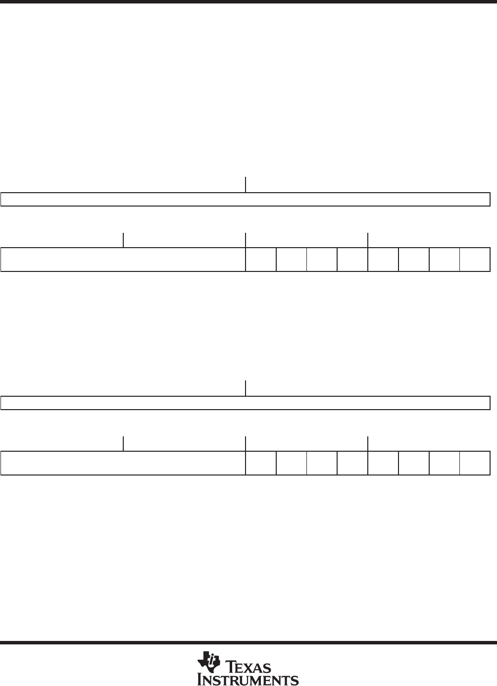
Figure 9 shows the GPIO enable bits in the GPEN register for the device. To use any of the GPx pins as
general-purpose input/output functions, the corresponding GPxEN bit must be set to “1” (enabled). Default
values are device-specific, so refer to Figure 9 for the default configuration.
31 24 23 16
Reserved
R-0
15 14 13 12 11
10 9 8 7 6543210
Reserved
GP7
EN
GP6
EN
GP5
EN
GP4
EN
—
GP2
EN
— —
R/W-0 R/W-1 R/W-1 R/W-1 R/W-1 R/W-0 R/W-0 R/W-0 R/W-0
Legend:
R/W = Readable/Writeable; -n = value after reset, -x = undefined value after reset
Figure 9. GPIO Enable Register (GPEN) [Hex Address: 01B0 0000]
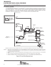
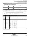
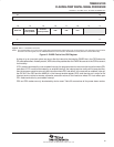
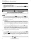
Figure 10 shows the GPIO direction bits in the GPDIR register. This register determines if a given GPIO pin is
an input or an output providing the corresponding GPxEN bit is enabled (set to “1”) in the GPEN register. By
default, all the GPIO pins are configured as input pins.
31 24 23 16
Reserved
R-0
15 14 13 12 11
10 9 8 7 6543210
Reserved
GP7
DIR
GP6
DIR
GP5
DIR
GP4
DIR
—
GP2
DIR
— —
R/W-0 R/W-0 R/W-0 R/W-0 R/W-0 R/W-0 R/W-0 R/W-0 R/W-0 R/W-0 R/W-0 R/W-0 R/W-0 R/W-0 R/W-0 R/W-0
Legend: R/W = Readable/Writeable; -n = value after reset, -x = undefined value after reset
Figure 10. GPIO Direction Register (GPDIR) [Hex Address: 01B0 0004]
For more detailed information on general-purpose inputs/outputs (GPIOs), see the TMS320C6000 DSP
General-Purpose Input/Output (GPIO) Reference Guide (literature number SPRU584).