TMS320C6712D
FLOATINGĆPOINT DIGITAL SIGNAL PROCESSOR
SPRS293A − OCTOBER 2005 − REVISED NOVEMBER 2005
43
POST OFFICE BOX 1443 • HOUSTON, TEXAS 77251−1443
interrupt sources and interrupt selector
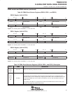
The C67x DSP core supports 16 prioritized interrupts, which are listed in Table 19. The highest priority interrupt
is INT_00 (dedicated to RESET) while the lowest priority is INT_15. The first four interrupts are non-maskable
and fixed. The remaining interrupts (4−15) are maskable and default to the interrupt source listed in Table 19.
However, their interrupt source may be reprogrammed to any one of the sources listed in Table 20 (Interrupt
Selector). Table 20 lists the selector value corresponding to each of the alternate interrupt sources. The selector
choice for interrupts 4−15 is made by programming the corresponding fields (listed in Table 19) in the MUXH
(address 0x019C0000) and MUXL (address 0x019C0004) registers.
Table 19. DSP Interrupts Table 20. Interrupt Selector
DSP
INTERRUPT
NUMBER
INTERRUPT
SELECTOR
CONTROL
REGISTER
DEFAULT
SELECTOR
VALUE
(BINARY)
DEFAULT
INTERRUPT
EVENT
INTERRUPT
SELECTOR
VALUE
(BINARY)
INTERRUPT
EVENT
MODULE
INT_00 − − RESET 00000 − −
INT_01 − − NMI 00001 TINT0 Timer 0
INT_02 − − Reserved 00010 TINT1 Timer 1
INT_03 − − Reserved 00011 SDINT EMIF
INT_04 MUXL[4:0] 00100 GPINT4
†
00100 GPINT4
†
GPIO
INT_05 MUXL[9:5] 00101 GPINT5
†
00101 GPINT5
†
GPIO
INT_06 MUXL[14:10] 00110 GPINT6
†
00110 GPINT6
†
GPIO
INT_07 MUXL[20:16] 00111 GPINT7
†
00111 GPINT7
†
GPIO
INT_08 MUXL[25:21] 01000 EDMAINT 01000 EDMAINT EDMA
INT_09 MUXL[30:26] 01001 EMUDTDMA 01001 EMUDTDMA Emulation
INT_10 MUXH[4:0] 00011 SDINT 01010 EMURTDXRX Emulation
INT_11 MUXH[9:5] 01010 EMURTDXRX 01011 EMURTDXTX Emulation
INT_12 MUXH[14:10] 01011 EMURTDXTX 01100 XINT0 McBSP0
INT_13 MUXH[20:16] 00000 DSPINT 01101 RINT0 McBSP0
INT_14 MUXH[25:21] 00001 TINT0 01110 XINT1 McBSP1
INT_15 MUXH[30:26] 00010 TINT1 01111 RINT1 McBSP1
10000 GPINT0 GPIO
†
Interrupt Events GPINT4, GPINT5, GPINT6, and GPINT7 are outputs from the GPIO module (GP). They originate from the device pins
GP[4](EXT_INT4), GP[5](EXT_INT5), GP[6](EXT_INT6), and GP[7](EXT_INT7). These pins can be used as edge-sensitive EXT_INTx
with polarity controlled by the External Interrupt Polarity Register (EXTPOL.[3:0]). The corresponding pins must first be enabled in the GPIO
module by setting the corresponding enable bits in the GP Enable Register (GPEN.[7:4]), and configuring them as inputs in the GP Direction
Register (GPDIR.[7:4]). These interrupts can be controlled through the GPIO module in addition to the simple EXTPOL.[3:0] bits. For more
information on interrupt control via the GPIO module, see the TMS320C6000 DSP General-Purpose Input/Output (GPIO) Reference Guide
(literature number SPRU584).


