TMS320C6712D
FLOATINGĆPOINT DIGITAL SIGNAL PROCESSOR
SPRS293A − OCTOBER 2005 − REVISED NOVEMBER 2005
60
POST OFFICE BOX 1443 • HOUSTON, TEXAS 77251−1443
EMIF big endian mode correctness
The device Endian mode pin (LENDIAN) selects the endian mode of operation (little endian or big endian) for
the device. Little endian is the default setting.
When Big Endian mode is selected (LENDIAN = 0), the EMIF Big Endian mode correctness pin (EMIFBE
) must
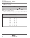
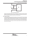
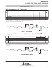
to be pulled low. Figure 14 shows the mapping of 16-bit and 8-bit data for the device with EMIF endianness
correction.
EMIF DATA LINES (PINS) WHERE DATA PRESENT
ED[15:8] (BE1) ED[7:0] (BE0)
16-Bit Device in Any Endianness Mode
8-Bit Device in Any Endianness Mode
Figure 14. 16/8-Bit EMIF Big Endian Mode Correctness Mapping]
This new feature does not affect systems operating in Little Endian mode, providing the default value of the C15
pin =1 is used.
bootmode
The C67x device resets using the active-low signal RESET and the internal reset signal. While RESET is low,
the internal reset is also asserted and the device is held in reset and is initialized to the prescribed reset state.
Refer to reset timing for reset timing characteristics and states of device pins during reset. The release of the
internal reset signal (see the Reset Phase 3 discussion in the Reset Timing section of this data sheet) starts
the processor running with the prescribed device configuration and boot mode.
The C6712D has two types of boot mode:
D Emulation boot
In Emulation boot mode, it is not necessary to load valid code into internal memory. The emulation driver will
release the CPU from the “stalled” state, at which point the CPU will vector to address 0. Prior to beginning
execution, the emulator sets a breakpoint at address 0. This prevents the execution of invalid code by
halting the CPU prior to executing the first instruction. Emulation boot is a good tool in the debug phase of
development.
D EMIF boot (using default ROM timings)
Upon the release of internal reset, the 1K-Byte ROM code located in the beginning of CE1
is copied to
address 0 by the EDMA using the default ROM timings, while the CPU is internally “stalled”. The data should
be stored in the endian format that the system is using. The boot process also lets you choose the width of
the ROM. In this case, the EMIF automatically assembles consecutive 8-bit bytes or 16-bit half-words to
form the 32-bit instruction words to be copied. The transfer is automatically done by the EDMA as a
single-frame block transfer from the ROM to address 0. After completion of the block transfer, the CPU is
released from the “stalled” state and starts running from address 0.
reset
A hardware reset (RESET) is required to place the DSP into a known good state out of power−up. The RESET
signal can be asserted (pulled low) prior to ramping the core and I/O voltages or after the core and I/O voltages
have reached their proper operating conditions. As a best practice, reset should be held low during power−up.
Prior to deasserting RESET
(low−to−high transition), the core and I/O voltages should be at their proper
operating conditions and CLKIN should also be running at the correct frequency.


