


TMS320C6712D
FLOATINGĆPOINT DIGITAL SIGNAL PROCESSOR
SPRS293A − OCTOBER 2005 − REVISED NOVEMBER 2005
3
POST OFFICE BOX 1443 • HOUSTON, TEXAS 77251−1443
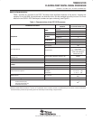
REVISION HISTORY
The TMS320C6712D device-specific documentation has been split from TMS320C6712, TMS320C6712C,
TMS320C6712D Floating−Point Digital Signal Processors, literature number SPRS148L, into a separate Data
Sheet, literature number SPRS293. It also highlights technical changes made to SPRS293 to generate
SPRS293A; these changes are marked by “[Revision A]” in the Revision History table below
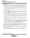
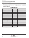
Scope: Updated information on McBSP and JTAG for clarification. Changed Pin Description for A12 and B11
(Revisions SPRS293 and SPRS293A). Updated Nomenclature figure by adding device−specific information for
the ZDP package. TI Recommends for new designs that the following pins be configured as such:
D Pin A12 connected directly to CV
DD
(core power)
D Pin B11 connected directly to V
ss
(ground)
PAGE(S)
NO.
ADDITIONS/CHANGES/DELETIONS
20 Device Configurations, device configurations at device reset section:
Added Note
25 Terminal Functions, Bootmode section:
Added Note
25 Terminal Functions, Little/Big Endian Format section:
Added Note
26 Terminal Functions, Resets and Interrupts section:
Updated IPU/IPD for RESET
Signal Name from “IPU” to “−−”
29 Terminal Functions, Reserved for Test section:
Changed “IPU” to “−−” for RSV C12
Changed “IPU” to “−−” for RSV D12
Updated Type for RSV D12 from “O” to “I”
30 Terminal Functions, Reserved for Test section:
Updated Description for RSV Signal Name, A12 GDP/ZDP
Updated Description for RSV Signal Name, B11 GDP/ZDP
30 Terminal Functions, Reserved for Test section:
Updated/changed Description for RSV Signal Name, A12 GDP (to “recommended”) − [Revision A]
Updated/changed Description for RSV Signal Name, B11 GDP (to “recommended”) − [Revision A]
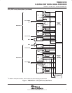
38 Device Support, device and development-support tool nomenclature:
Updated figure for clarity
39 Device Support, document support section:
Updated paragraphs for clarity
58 IEEE 1149.1 JTAG Compatibility Statement section:
Updated/added paragraphs for clarity
61 Recommended Operating Conditions:
Added V
OS,
Maximum voltage during overshoot row and associated footnote
Added V
US,
Maximum voltage during undershoot row and associated footnote
64 Parameter Measurement Information:
AC transient rise/fall time specifications section:
Added AC Transient Specification Rise Time figure
Added AC Transient Specification Fall Time figure