TMS320C6712D
FLOATINGĆPOINT DIGITAL SIGNAL PROCESSOR
SPRS293A − OCTOBER 2005 − REVISED NOVEMBER 2005
84
POST OFFICE BOX 1443 • HOUSTON, TEXAS 77251−1443
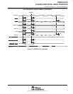
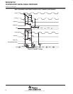
RESET TIMING (CONTINUED)
Phase 1 Phase 2
11
10
9
87
65
43
13
12
2
11
CLKIN
ECLKIN
Internal Reset
Internal SYSCLK1
Internal SYSCLK2
Internal SYSCLK3
RESET
Phase 3
EMIF Z Group
†
EMIF Low Group
†
Z Group
†
Boot
and
Device
Configuration
Pins‡
2
2
2
CLKOUT3
ECLKOUT
CLKOUT2
†
EMIF Z group consists of: EA[21:2], ED[15:0], CE[3:0]
, BE[1:0], ARE/SDCAS/SSADS, AWE/SDWE/SSWE, AOE/SDRAS/SSOE and
HOLDA
EMIF low group consists of: BUSREQ
Z group consists of: CLKR0, CLKR1, CLKX0, CLKX1, FSR0, FSR1, FSX0, FSX1, DX0, DX1, TOUT0, and TOUT1.
‡
Boot and device configurations consist of: BOOTMODE[1:0] and LENDIAN.
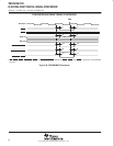
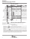
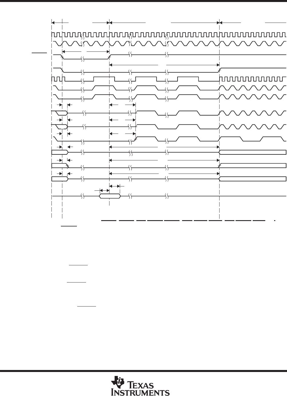
Figure 39. Reset Timing
Reset Phase 1: The RESET
pin is asserted. During this time, all internal clocks are running at the CLKIN
frequency divide-by-8. The CPU is also running at the CLKIN frequency divide-by-8.
Reset Phase 2: The RESET
pin is deasserted but the internal reset is stretched. During this time, all internal
clocks are running at the CLKIN frequency divide-by-8. The CPU is also running at the CLKIN frequency
divide-by-8.
Reset Phase 3: Both the RESET pin and internal reset are deasserted. During this time, all internal clocks are
running at their default divide-down frequency of CLKIN. The CPU clock (SYSCLK1) is running at CLKIN
frequency. The peripheral clock (SYSCLK2) is running at CLKIN frequency divide-by-2. The EMIF internal clock
source (SYSCLK3) is running at CLKIN frequency divide-by-2. SYSCLK3 is reflected on the ECLKOUT pin
(when EKSRC bit = 0 [default]). CLKOUT3 is running at CLKIN frequency divide-by-8.


