


TMS320C6712D
FLOATINGĆPOINT DIGITAL SIGNAL PROCESSOR
SPRS293A − OCTOBER 2005 − REVISED NOVEMBER 2005
40
POST OFFICE BOX 1443 • HOUSTON, TEXAS 77251−1443
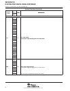
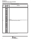
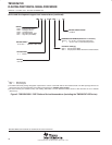
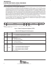
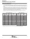
CPU CSR register description
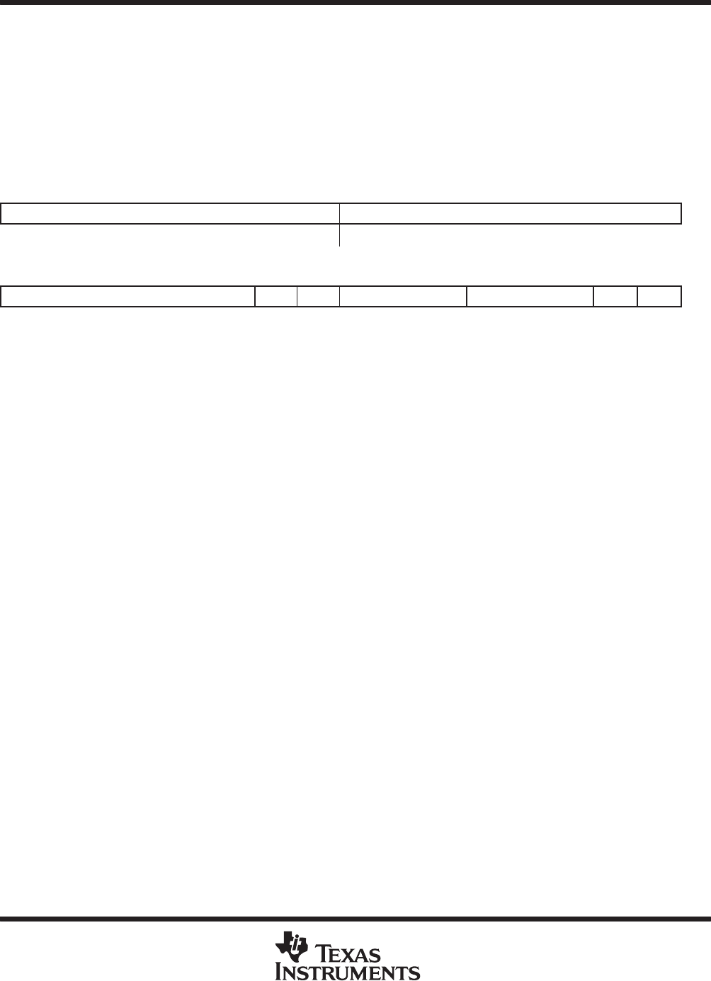
The CPU control status register (CSR) contains the CPU ID and CPU Revision ID (bits 16−31) as well as the
status of the device power-down modes [PWRD field (bits 15−10)], program and data cache control modes, the
endian bit (EN, bit 8) and the global interrupt enable (GIE, bit 0) and previous GIE (PGIE, bit 1). Figure 6 and
Table 17 identify the bit fields in the CPU CSR register.
For more detailed information on the bit fields in the CPU CSR register, see the TMS320C6000 DSP Peripherals
Overview Reference Guide (literature number SPRU190) and the TMS320C6000 CPU and Instruction Set
Reference Guide (literature number SPRU189).
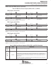
31 24 23 16
CPU ID REVISION ID
R-0x02 R-0x03
15 10 9 8 7 6 5 4 2 1 0
PWRD
SAT EN PCC DCC PGIE GIE
R/W-0 R/C-0 R-1 R/W-0 R/W-0 R/W-0 R/W-0
Legend:
R = Readable by the MVC instruction, R/W = Readable/Writeable by the MVC instruction; W = Read/write; -n = value after reset, -x = undefined value after
reset, C = Clearable by the MVC instruction
Figure 6. CPU Control Status Register (CPU CSR)