


TMS320C6712D
FLOATINGĆPOINT DIGITAL SIGNAL PROCESSOR
SPRS293A − OCTOBER 2005 − REVISED NOVEMBER 2005
47
POST OFFICE BOX 1443 • HOUSTON, TEXAS 77251−1443
PLL and PLL controller (continued)
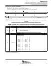
The PLL Reset Time is the amount of wait time needed when resetting the PLL (writing PLLRST=1), in order
for the PLL to properly reset, before bringing the PLL out of reset (writing PLLRST = 0). For the PLL Reset Time
value, see Table 25. The PLL Lock Time is the amount of time from when PLLRST = 0 with PLLEN = 0 (PLL
out of reset, but still bypassed) to when the PLLEN bit can be safely changed to “1” (switching from bypass to
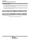
the PLL path), see Table 25 and Figure 8.
Under some operating conditions, the maximum PLL Lock Time may vary from the specified typical value. For
the PLL Lock Time values, see Table 25.
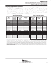
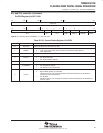
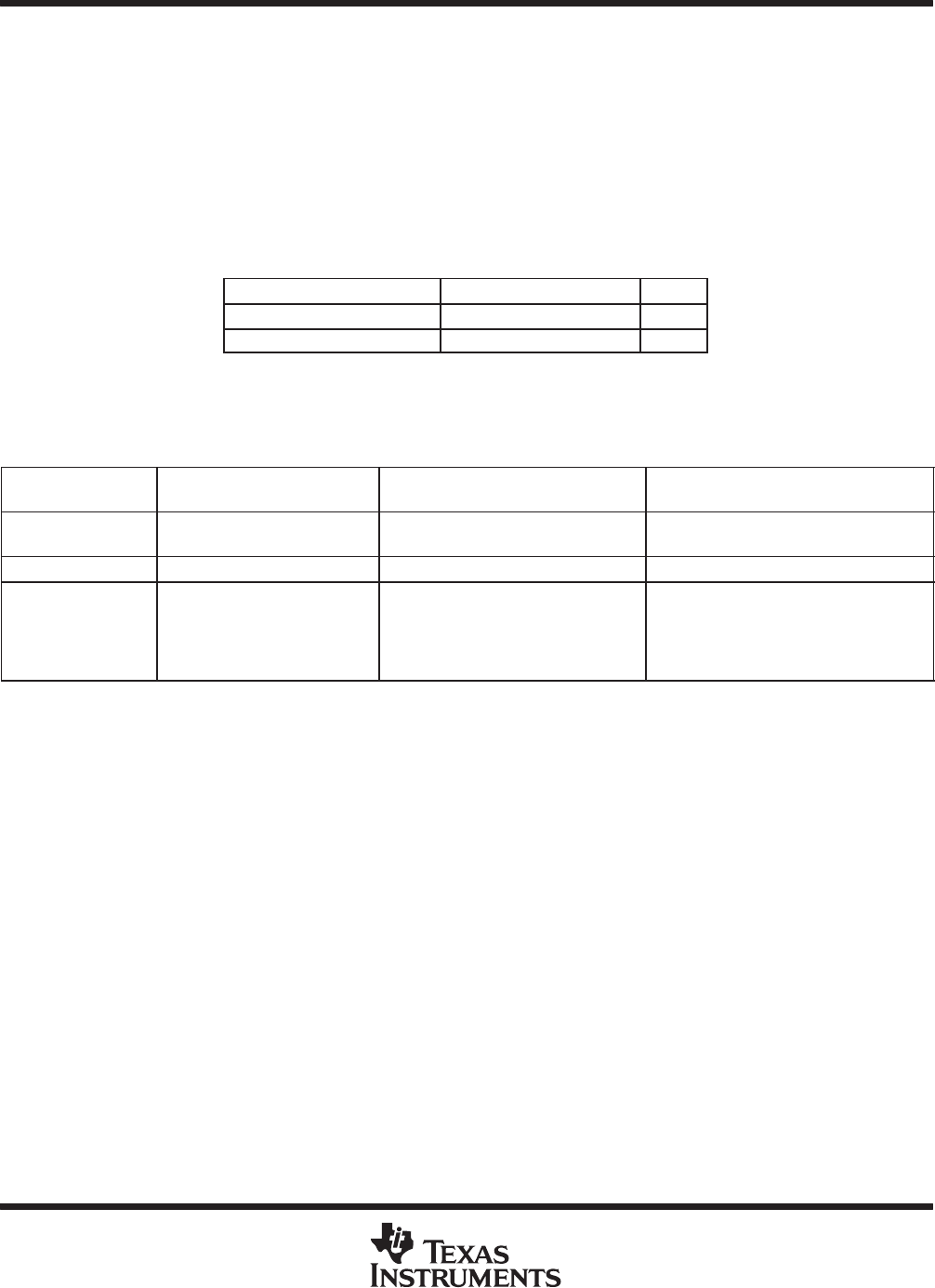
Table 25. PLL Lock and Reset Times
MIN TYP MAX UNIT
PLL Lock Time 75 187.5 µs
PLL Reset Time 125 ns
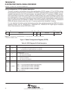
Table 26 shows the device’s CLKOUT signals, how they are derived and by what register control bits, and the
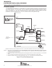
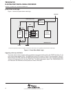
default settings. For more details on the PLL, see the PLL and Clock Generator Logic diagram (Figure 8).
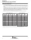
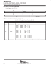
Table 26. CLKOUT Signals, Default Settings, and Control
CLOCK OUTPUT
SIGNAL NAME
DEFAULT SETTING
(ENABLED or DISABLED)
CONTROL
BIT(s) (Register)
DESCRIPTION
CLKOUT2 ON (ENABLED)
D2EN = 1 (PLLDIV2.[15])
CK2EN = 1 (EMIF GBLCTL.[3])
SYSCLK2 selected [default]
CLKOUT3 ON (ENABLED) OD1EN = 1 (OSCDIV1.[15]) Derived from CLKIN
ECLKOUT
ON (ENABLED);
derived from SYSCLK3
EKSRC = 0 (DEVCFG.[4])
EKEN = 1 (EMIF GBLCTL.[5])
SYSCLK3 selected [default].
To select ECLKIN as source:
EKSRC = 1 (DEVCFG.[4]) and
EKEN = 1 (EMIF GBLCTL.[5])
This input clock is directly available as an internal high-frequency clock source that may be divided down by
a programmable divider OSCDIV1 (/1, /2, /3, ..., /32) and output on the CLKOUT3 pin for other use in the system.
Figure 8 shows that the input clock source may be divided down by divider PLLDIV0 (/1, /2, ..., /32) and then
multiplied up by a factor of x4, x5, x6, and so on, up to x25.
Either the input clock (PLLEN = 0) or the PLL output (PLLEN = 1) then serves as the high-frequency reference
clock for the rest of the DSP system. The DSP core clock, the peripheral bus clock, and the EMIF clock may
be divided down from this high-frequency clock (each with a unique divider) . For example, with a 40-MHz input,
if the PLL output is configured for 300 MHz, the DSP core may be operated at 150 MHz (/2) while the EMIF may
be configured to operate at a rate of 60 MHz (/5). Note that there is a specific minimum and maximum reference
clock (PLLREF) and output clock (PLLOUT) for the block labeled PLL in Figure 8, as well as for the DSP core,
peripheral bus, and EMIF. The clock generator must not be configured to exceed any of these constraints
(certain combinations of external clock input, internal dividers, and PLL multiply ratios might not be supported).
See Table 27 for the PLL clocks input and output frequency ranges.