


CY7C67200
Document #: 38-08014 Rev. *G Page 39 of 78
OTG Control Registers
There is one register dedicated for OTG operation. This
register is covered in this section and summarized in Ta ble 28.
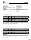
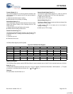
OTG Control Register [0xC098] [R/W]
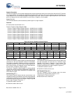
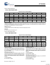
Figure 40. OTG Control Register
Register Description
The OTG Control register allows control and monitoring over
the OTG port on Port1A.
VBUS Pull-up Enable (Bit 13)
The VBUS Pull-up Enable bit enables or disables a 500 ohm
pull-up resistor onto OTG VBus.
1: 500 ohm pull-up resistor enabled
0: 500 ohm pull-up resistor disabled
Receive Disable (Bit 12)
The Receive Disable bit enables or powers down (disables)
the OTG receiver section.
1: OTG receiver powered down and disabled
0: OTG receiver enabled
Charge Pump Enable (Bit 11)
The Charge Pump Enable bit enables or disables the OTG
VBus charge pump.
1: OTG VBus charge pump enabled
0: OTG VBus charge pump disabled
VBUS Discharge Enable (Bit 10)
The VBUS Discharge Enable bit enables or disables a 2K-ohm
discharge pull-down resistor onto OTG VBus.
1: 2K-ohm pull-down resistor enabled
0: 2K-ohm pull-down resistor disabled
D+ Pull-up Enable (Bit 9)
The D+ Pull-up Enable bit enables or disables a pull-up
resistor on the OTG D+ data line.
1: OTG D+ dataline pull-up resistor enabled
0: OTG D+ dataline pull-up resistor disabled
D– Pull-up Enable (Bit 8)
The D– Pull-up Enable bit enables or disables a pull-up
resistor on the OTG D– data line.
1: OTG D– dataline pull-up resistor enabled
0: OTG D– dataline pull-up resistor disabled
D+ Pull-down Enable (Bit 7)
The D+ Pull-down Enable bit enables or disables a pull-down
resistor on the OTG D+ data line.
1: OTG D+ dataline pull-down resistor enabled
0: OTG D+ dataline pull-down resistor disabled
D– Pull-down Enable (Bit 6)
The D– Pull-down Enable bit enables or disables a pull-down
resistor on the OTG D– data line.
1: OTG D– dataline pull-down resistor enabled
0: OTG D– dataline pull-down resistor disabled
OTG Data Status (Bit 2)
The OTG Data Status bit is a read only bit and indicates the
TTL logic state of the OTG VBus pin.
1: OTG VBus is greater than 2.4V
0: OTG VBus is less than 0.8V
ID Status (Bit 1)
The ID Status bit is a read only bit that indicates the state of
the OTG ID pin on Port A.
1: OTG ID Pin is not connected directly to ground (>10K ohm)
0: OTG ID Pin is connected directly ground (< 10 ohm)
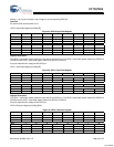
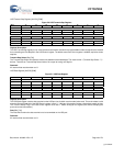
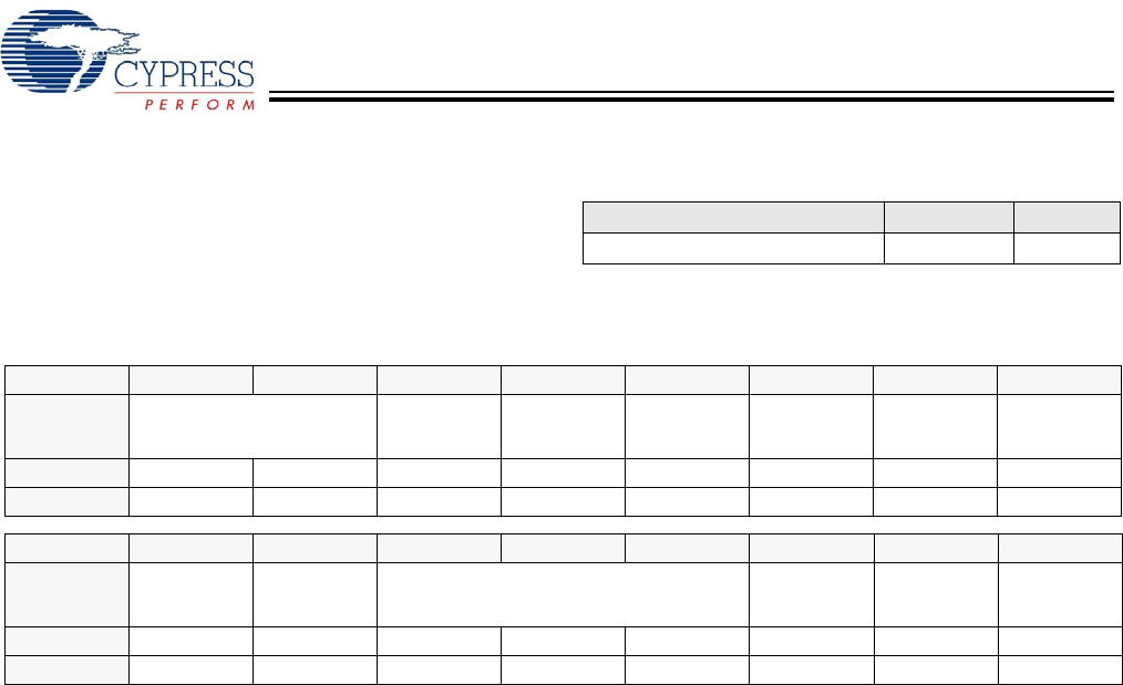
Table 28.OTG Registers
Register Name Address R/W
OTG Control Register C098H R/W
Bit # 15 14 13 12 11 10 9 8
Field Reserved VBUS
Pull-up
Enable
Receive
Disable
Charge Pump
Enable
VBUS
Discharge
Enable
D+
Pull-up
Enable
D–
Pull-up
Enable
Read/Write - - R/W R/W R/W R/W R/W R/W
Default 0 0 0 0 0 0 0 0
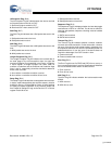
Bit # 7 6 5 4 3 2 1 0
Field D+
Pull-down
Enable
D–
Pull-down
Enable
Reserved OTG Data
Status
ID
Status
VBUS Valid
Flag
Read/Write R/W R/W - - - R R R
Default 0 0 0 0 0 X X X
[+] Feedback